


© 2024 EasyEDA Some rights reserved ISO/IEC
Editor Version
×
Standard

1.Easy to use and quick to get started
2.The process supports design scales of 300 devices or 1000 pads
3.Supports simple circuit simulation
4.For students, teachers, creators
Profession

1.Brand new interactions and interfaces
2.Smooth support for design sizes of over 5,000 devices or 10,000 pads
3.More rigorous design constraints, more standardized processes
4.For enterprises, more professional users
Ongoing
STD Digital Circuit - Experimental Platform by JLCPCB
Mode: Editors' pick
- 0
Update time:
2020-05-07 09:56:23
Creation time:
2020-04-28 08:31:50
Description
Digital Circuit - Experimental Platform by [JLCPCB](JLCPCB)
The Digital circuit experimental board is a set of small and delicate experimental boards designed by [JLCPCB](JLCPCB) and [LCSC](LCSC )to adapt to digital circuit experiments. The board uses Micro USB 5V input, can use mobile power, phone charger, computer, and other electrical appliances with USB interface for power supply, easy to carry, adapt to a variety of teaching environments.
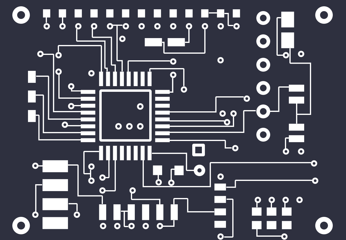
1 The size of the board is 10cm*8cm which consists of the Onboard power control module, LED level display module, digital tube display module, a level selection module, single pulse generation module, 555 square wave generation module, and IC socket module, circuit PCB preview show as below;

Step 1: Power Control Module
Power Control Module
The experimental board uses an embedded micro USB interface for power supply, which is easy for welding and provides power in a variety of ways. After power connected, a dial switch is used to control the on and off of the total power supply. When the power is on, LED10 red light is on, and the power supply works normally. The schematic diagram of the circuit is as follows

Step 2: Level Indicator Module
Level Indicator Module
This part adopts 8 groups of audions to drive an LED circuit, which is connected to the outside to conduct the triode at high voltage and light up the LED; When low power is connected, the triode is disconnected and the LED is extinguished. The schematic diagram of the circuit shown as follows;

Step 3: LED Display Module
LED Display Module
The digital tube display circuit adopts an eight-segment cathode digital tube, which is connected with current limiting resistance. When the input is a high voltage, the corresponding segment of the digital tube is lit up, while the input is low voltage, the circuit is turned off. The schematic as below;

Step 4: Level Option Module
Level Option Module
The experimental board provides eight levels output, using a dial switch to control the output, according to the silkscreen, dial to the right when the output of high level, or vice versa, schematic as below; If you need to change the schematic, click EasyEDA

Step 5: Single Pulse Module
Single Pulse Module
The experimental board provides two opposite mono Pulse Generator, NAND gate, and a dial switch combine a RS Generator. The two output states are opposite, and the two output states are changed simultaneously by the dial switch. The schematic as below;If you need to change the schematic, click EasyEDA

Step 6: 555 Pulse Generator Module
555 Pulse Generator Module
The board provides an adjustable square pulse frequency between 10KHZ and 40KHZ that can be used as the clock input, and the output frequency is regulated by a potentiometer, the schematic as below; If you need to change the schematic, click EasyEDA

Step 7: IC Socket Module
In order to adapt to the functional verification of a variety of chips, two DIP14 sockets are provided on the experimental board, in which the seventh pin is connected with GND by default, the 14th pin is connected with VCC by default, and the other pins respectively lead out two-row pins for use.

There are also two DIP16 sockets. The corresponding eighth and 16th pins are connected with GND and VCC respectively. The rest pins also lead to two rows of pins. In addition, some of the pin arrangement of the chip is irregular, and a DIP20 socket is provided on the board. This socket is not connected with GND and VCC, and is connected according to the pin arrangement of the chip in the experiment; The schematic is below. If you need to change the schematic, click EasyEDA


Design Drawing
schematic diagram
(
1
/
)
PCB
(
1
/
)
The preview image was not generated, please save it again in the
editor.
BOM
Project Members


 0
0
 0
0
Collect to album
Target complaint
Related Projects
Change a batch
Loading...
Add to album
×
Loading...
reminder
×
Do you need to add this project to the album?