


© 2024 EasyEDA Some rights reserved ISO/IEC
Editor Version
×
Standard

1.Easy to use and quick to get started
2.The process supports design scales of 300 devices or 1000 pads
3.Supports simple circuit simulation
4.For students, teachers, creators
Profession

1.Brand new interactions and interfaces
2.Smooth support for design sizes of over 5,000 devices or 10,000 pads
3.More rigorous design constraints, more standardized processes
4.For enterprises, more professional users

Ongoing
STD Nixie_clock_hw
License: BSD
Mode: Editors' pick
- 1
Update time:
2023-03-31 07:10:53
Creation time:
2019-07-13 06:13:01
Description
IN14 Nixie tube block
Design Drawing
schematic diagram
(
1
/
)
-

Leds.ascii
Open in Editor -

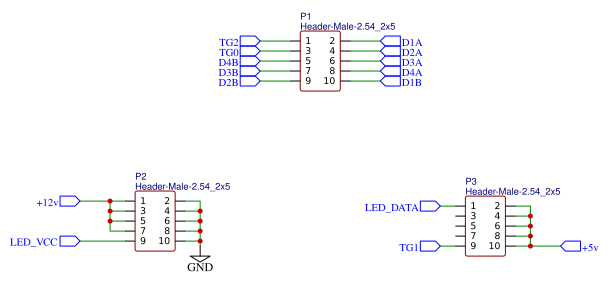
connectors
Open in Editor -

170v DCDC
Open in Editor -

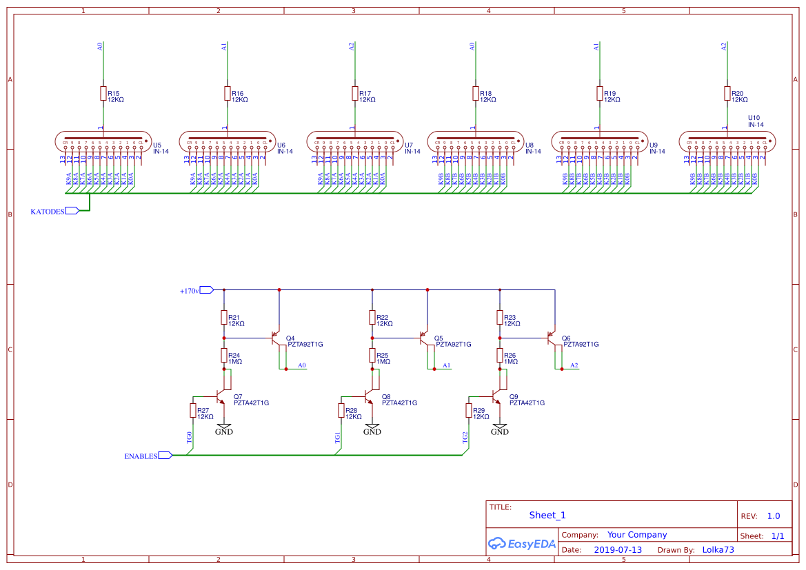
Tubes
Open in Editor -

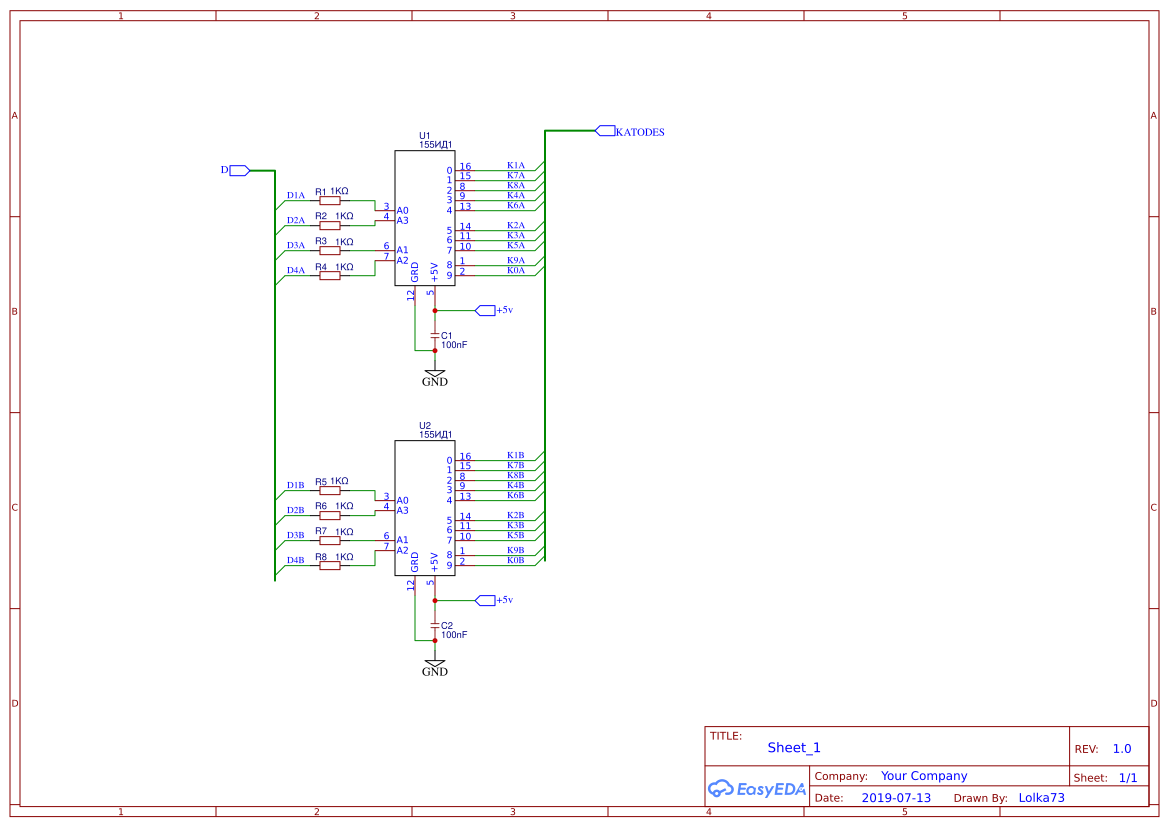
Decoders
Open in Editor
PCB
(
1
/
)
The preview image was not generated, please save it again in the
editor.
| ID | Name | Designator | Footprint | Quantity |
|---|---|---|---|---|
| 1 | 100nF | C1,C2,C11,C13 | C0805 | 4 |
| 2 | 1KΩ | R1,R2,R3,R4,R5,R6,R7,R8 | 0805 | 8 |
| 3 | 155ИД1 | U1,U2 | DIP16_SMD | 2 |
| 4 | WS2812B | LED1,LED2,LED3,LED4,LED5,LED6 | LED-5050_4P | 6 |
| 5 | 10kΩ | R9 | 0805 | 1 |
| 6 | Header-Male-2.54_2x5 | P1,P2,P3 | HDR-5X2/2.54 | 3 |
| 7 | 4.7uF | C9 | CAP-D10.0XF5.0 | 1 |
| 8 | 220nF | C10 | CAP-CBB-13.0*4.0 | 1 |
| 9 | 470pF | C12 | C0805 | 1 |
| 10 | HER106 | D1 | DO214AC | 1 |
| 11 | 330uH | L1 | L1010 | 1 |
| 12 | BC847 | Q1 | SOT23-3 | 1 |
| 13 | IRF840S | Q2 | D2PAK | 1 |
| 14 | BC857 | Q3 | SOT23-3 | 1 |
| 15 | 0.22Ω | R10 | RESISTOR CERAMIC BPR56 | 1 |
| 16 | 1MΩ | R11,R24,R25,R26 | 0805 | 4 |
| 17 | 330Ω | R12,R14 | 0805 | 2 |
| 18 | 5.1KΩ | R13 | 0805 | 1 |
| 19 | 1.5KΩ | R30 | 0805 | 1 |
| 20 | 300k | U3 | TC33X | 1 |
| 21 | MC34063ADR | U4 | SOIC-8_150MIL | 1 |
| 22 | PZTA92T1G | Q4,Q5,Q6 | SOT-223 | 3 |
| 23 | PZTA42T1G | Q7,Q8,Q9 | SOT-223 | 3 |
| 24 | 12KΩ | R15,R16,R17,R18,R19,R20,R21,R22,R23,R27,R28,R29 | 0805 | 12 |
| 25 | IN-14 | U5,U6,U7,U8,U9,U10 | IN14_PCB | 6 |
Unfold
Project Members


 0
0
 1
1
Collect to album
Target complaint
Related Projects
Change a batch
Loading...
Add to album
×
Loading...
reminder
×
Do you need to add this project to the album?