


© 2024 EasyEDA Some rights reserved ISO/IEC
Editor Version
×
Standard

1.Easy to use and quick to get started
2.The process supports design scales of 300 devices or 1000 pads
3.Supports simple circuit simulation
4.For students, teachers, creators
Profession

1.Brand new interactions and interfaces
2.Smooth support for design sizes of over 5,000 devices or 10,000 pads
3.More rigorous design constraints, more standardized processes
4.For enterprises, more professional users
Ongoing
STD FabTester
License: Public Domain
Mode: Editors' pick
- 0
Update time:
2021-04-11 23:44:59
Creation time:
2017-03-28 19:51:41
Description
A small, basic fab capability checker.
- Board edge cutouts
- Text on copper and silkscreen layer
- 20 to 5 mil traces for silkscreen, both straight and curved
- Silkscreen-to-footprint alignment
- Through-hole accuracy
- Via centered drill check
- Complex footprint check
- Ground plane check
- Ground plane connectivity check
Design Drawing
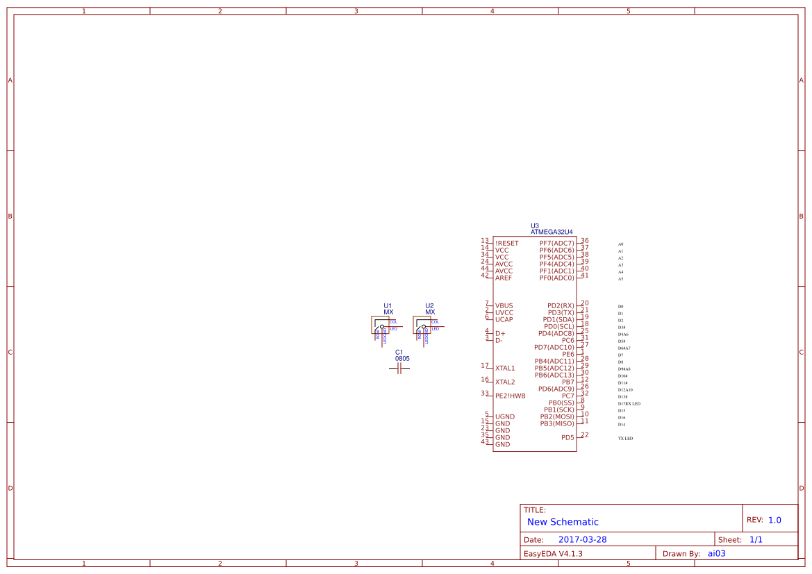
schematic diagram
(
1
/
)
PCB
(
1
/
)
The preview image was not generated, please save it again in the
editor.
| ID | Name | Designator | Footprint | Quantity |
|---|---|---|---|---|
| 1 | MX | U1,U2 | Cherry MX + Alps 1U | 2 |
| 2 | ATMEGA32U4 | U3 | SPARKFUN-DIGITALIC_TQFP44 | 1 |
| 3 | 0805 | C1 | 0805-ExtendedPads-MarkedBorders | 1 |
Unfold
Project Members


 0
0
 0
0
Collect to album
Target complaint
Related Projects
Change a batch
Loading...
Add to album
×
Loading...
reminder
×
Do you need to add this project to the album?