


© 2024 EasyEDA Some rights reserved ISO/IEC
Editor Version
×
Standard

1.Easy to use and quick to get started
2.The process supports design scales of 300 devices or 1000 pads
3.Supports simple circuit simulation
4.For students, teachers, creators
Profession

1.Brand new interactions and interfaces
2.Smooth support for design sizes of over 5,000 devices or 10,000 pads
3.More rigorous design constraints, more standardized processes
4.For enterprises, more professional users
Ongoing
STD Castellated hole bug
License: Public Domain
Mode: Editors' pick
- 1
Update time:
2021-04-11 20:32:45
Creation time:
2018-01-02 21:04:57
Description
Project to more clearly demonstrate the bug identified in:
https://easyeda.com/forum/topic/Half_cut_Castellated_Holes_Not_Working-NQEeO0mjh
View the Gerber Output of this PCB in the EasyEDA Gerber Viewer at:
https://gerber-viewer.easyeda.com/?ref=easyeda.com#!id=2b0290f5f00211e79ed5026a86b9cae7
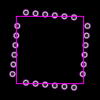
![enter image description here][1]
Note that all holes with centres outside of the left and bottom edges of the board outline are rendered offset from the pad centres.
Compare with the Gerber Output from this project when viewed in gerbv which is OK:
![enter image description here][2]
[1]: /editor/20180103/5a4bf9aca0d70.png
[2]: /editor/20180103/5a4bf95d791be.PNG
Design Drawing
schematic diagram
(
1
/
)
PCB
(
1
/
)
The preview image was not generated, please save it again in the
editor.
BOM
Project Members


 0
0
 1
1
Collect to album
Target complaint
Related Projects
Change a batch
Loading...
Add to album
×
Loading...
reminder
×
Do you need to add this project to the album?