


© 2024 EasyEDA Some rights reserved ISO/IEC
Editor Version
×
Standard

1.Easy to use and quick to get started
2.The process supports design scales of 300 devices or 1000 pads
3.Supports simple circuit simulation
4.For students, teachers, creators
Profession

1.Brand new interactions and interfaces
2.Smooth support for design sizes of over 5,000 devices or 10,000 pads
3.More rigorous design constraints, more standardized processes
4.For enterprises, more professional users
Ongoing
STD Essential checks before placing a PCB order
License: Public Domain
Mode: Editors' pick
- 3
Update time:
2020-07-28 01:44:43
Creation time:
2017-09-05 21:31:43
Description
Updated 181120
**A simple mistake can make a batch of PCBs useless so before submitting an order for PCBs, there are a lot of things to check.**
The list below is a good starting point for the essentials but it by no means exhaustive!
1) Check that all nets and netnames are as intended. For example nets can be accidentally connected together while drawing and editing a schematic and also by inadvertently assigning duplicated netlabels;
2) Check that the appropriate package has been assigned to each and every schematic symbol. Don't forget that different transistors, capacitors and even resistors may be in different packages in different locations in a schematic. Also check that components have been rated correctly as this may affect their package size (don't forget their height too!);
3) Check that the pin designations of the schematic symbol and the PCB package are the same. The pins on the schematic symbol for a bipolar transistor may be labelled B, C, and E but if the corresponding pins on the PCB footprint are labelled as 1, 2, and 3 then EasyEDA will flag this as an error when an attempt is made to convert the schematic into a PCB. It is simple to correct or - better - avoid this: change the labelling on the corresponding pins of the PCB footprint to B, C and E **or** change the labelling on the corresponding pins of the schematic symbol to 1, 2 and 3.
To change the pin labelling in the schematic to match the PCB footprint: select the part, press the `i` key then edit the **Names** in the **Edit Pin Map Information** section of the **Modify symbol information** dialogue that opens and click `OK` when finished.
To change the pin labelling in the PCB to match the schematic symbol: select each pin of the relevant part, then edit the pin **Names** in the right hand **Properties** panel.
Note: do not confuse the schematic symbol pin numbering with the spice pins numbering. For more about this see:
**Schematic symbols: prefixes and pin numbers** in:
https://docs.google.com/document/u/1/d/1OWZVVFRAe_2NW3WratpkA_SGuHa5AcRow5ZRfvcoVTU/pub#h.pkwqa1
4) Check that the pin designations of the PCB footprint chosen for each and every device actually matches the pinout of the device that will be soldered to it. It is very easy to assign a SOT23 package to a BC846 bipolar transistor where the pin order is:
Pin 1 = Base
Pin 2 = Emitter
Pin 3 = Collector
and then to forget that the pin order for a MMBF5485 junction FET going round the same SOT23 package in the same order is:
Pin 1 = Drain
Pin 2 = Source
Pin 3 = Gate
To change the pin labelling in the schematic to match the PCB footprint: select the part, press the `i` key then edit the order of the **PCB Pin** information in the **Edit Pin Map Information** section of the **Modify symbol information** dialogue that opens and click `OK` when finished.
To change the pin labelling in the PCB to match the schematic symbol: select each pin of the relevant part, then edit the pin **Numbers** in the right hand **Properties** panel.
5) Check that all necessary Bill of Materials (BoM) information is present and correct. Correct it and add more if required, making sure that fields such as `Description` are consistently labelled so that they form a coherent column structure in the BoM;
6) Check that all PCB footprints are correct for the intended devices (yes: whether they have come from the library or you have created them yourself: check them thoroughly);
7) Check that silkscreen markings such as the polarity markings for electrolytic capacitors and diodes are the right way round. Even if the pin names, numbering and sequence around tha package are correct, it can all go wrong if the footprint markings show the device in the wrong orientation.
9) Check that devices have been placed on the correct side of the board;
10) Refresh and check all the Components and Nets in the schematic Design Manager tab in the right hand panel;
11) Refresh and check all the Components, Nets and DRC Errors in the PCB Design Manager tab in the right hand panel;
12) Check connector and on-board pot and switch orientations;
13) Check the dimensions and locations of mounting holes and any components that have to line up with respect to these mounting holes or to apertures in an enclosure;
14) Check that the order of the top and bottom (and any inner layers) is correct;
15) Check that a Board Outline exists, is closed and that it is shaped and dimensioned correctly and is on the correct (Board Outline) layer;
16) Check that silkscreen markings do not overlap pads;
17) Check that all required silkscreen markings are present, in the correct locations on the correct layers, are within the recommended dimensions, are legible and and spelled correctly;
18) Check that any additional information such as notes about the PCB stackup etc., are present and on the correct (Documentation) layer;
19) Check that no board outline, silkscreen or documentation layer information has accidentally been placed on any copper layers;
20) Having completed the layout, check that the assembled component heights do not foul any enclosure (At the time of writing (160922) this is not something that can be acheived directly in EasyEDA as there is no 3D viewer yet available so this must be checked by other means);
21) Especially before generating the Gerber files, all copper areas must be rebuilt.
22) If copper areas are used with heat shunt spokes enabled, check that any tracks that join pins that are also joined by copper areas run within the area of a spoke. If they do not - for example a 45 degree diagonal track coming out of a pad with 90 degree heat shunt spokes - the track forms an extra spoke which increases the heat shunting to a pad and so may make soldering more difficult;
23) Check that all copper areas are assigned to a net. Do not let copper areas 'float' by leaving their `Net` attribute unassigned. If a copper area has no particular net associated with it it is usually best to assign it to ground or possibly to a supply rail.
24) Check that all copper areas assigned to a net are joined to each other by reasonable widths of copper, i.e. they are not just joined by thin slivers of copper;
25) Check that any tracks and Copper Areas that require special routing considerations such as Kelvin connections to low value current sense resistors or increased clearances for high voltage traces have been correctly implemented. Don't forget to check this after rebuilding Copper Areas;
26) Check clearances of copper on all layers and components on both sides to the edges of the board;
27) Use the Design Manager (the **Design** button in the left hand panel) to check that no traces have been set to hidden in the Design Manager Nets list;
28) Use the Design Manager (the **Design** button in the left hand panel) to check that all components are present in both the schematic and the PCB and that all nets have at least two connections;
29) Use the Design Manager (the **Design** button in the left hand panel) to check, investigate and correct all DRC errors.
A completed PCB design should have no DRC errors;
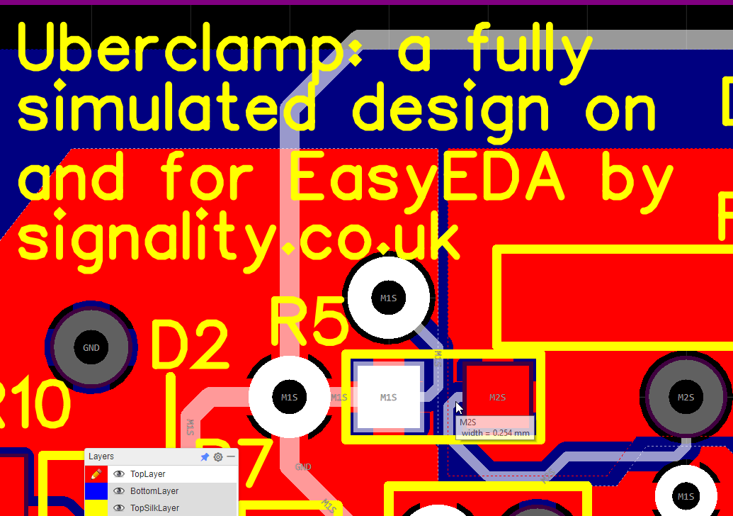
30) Before generating the Gerbers all copper areas must be rebuilt and checked. **Particular care is needed where the netnames of track segments in the PCB have been temporarily changed, for example to help in the creation of tracks for Kelvin connections to pads that are surrounded by a copper area which would normally swamp the tracks if their net names were left unchanged at the time the copper area was built or rebuilt. Such temporary segment net name changes must be made before building or rebuilding the surrounding copper area(s) but should be reset to their parent net names after building or rebuilding the surrounding copper area(s).**
An example of the creation of Kelvin connections using this technique can be seen in the close-up image below of the M1S and M2S nets in the [Uberclamp Project](https://easyeda.com/example/Uberclamp_Schematic_PCB_and_BoM-r4YgysK2k):
31) Run **Update PCB...** from the Schematic Editor or **Import Changes...** from the PCB Editor to do a final check that the PCB is up to date with the schematic. This is the simplest way to check for errors such as accidental changes to footprints assigned to schematic symbols or placed in the PCB and changes to net names that have been made to the PCB but which have not been made by changing the schematic first and then updating the PCB with the changes. If there are no differences between the schematic and PCB then **Update PCB...** or **Import Changes...** will return a message to show that they are the same. If there are differences then the tools will list them and it is then up to the user to either accept the changes that the tools will make to update the PCB or to cancel the update and make whatever changes are needed to achieve a "Schematic and PCB are the same" message if the **Update PCB...** or **Import Changes...** tool is rerun without accepting the changes. **Particular care is needed where the netnames of track segments in the PCB have been temporarily changed, for example to help in the creation of tracks for Kelvin connections to pads that are surrounded by a copper area which would normally swamp the tracks if their net names were left unchanged at the time the copper area was built or rebuilt. Such temporary segment net name changes must be made before building or rebuilding the surrounding copper area(s) but should be reset to their parent net names after building or rebuilding the surrounding copper area(s).**
32) Check that the Gerbers to be generated are from the correct version of the PCB layout. It may have changed as a result of the above checks so always regenerate the Gerbers from the latest version unless there is a specific reason to use them from an earlier version. Putting a version number on the PCB helps but is not perfect as this has to be updated manually anyway;
33) Download and check items (6) to (26) in the Gerbers in either the EasyEDA Gerber Viewer:
https://gerber-viewer.easyeda.com/
or using a 3rd party Gerber viewer such as the free and open source gerbv:
https://sourceforge.net/projects/gerbv/files/gerbv/
34) Check the order options such as number of boards, copper finish, silkscreen colour, solder mask colour, panellisation, any solder paste mask requirement and so on;
35) Lastly, check that the order is being placed with the correct delivery option. The default delivery method is by express courier. This is the most expensive option but avoids the mistake of ordering boards that are needed urgently with a slow delivery method.
Design Drawing
schematic diagram
(
1
/
)
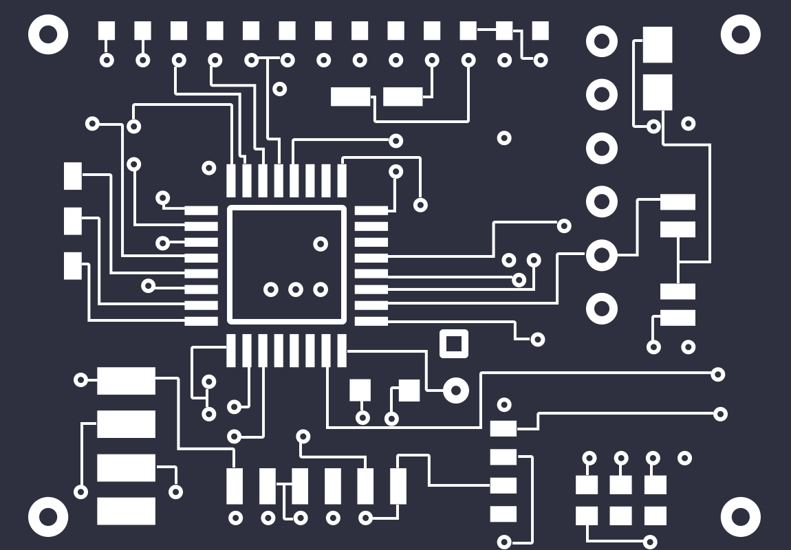
PCB
(
1
/
)
The preview image was not generated, please save it again in the
editor.
BOM
Project Members


 0
0
 3
3
Collect to album
Target complaint
Related Projects
Change a batch
Loading...
Add to album
×
Loading...
reminder
×
Do you need to add this project to the album?