


© 2024 EasyEDA Some rights reserved ISO/IEC
Editor Version
×
Standard

1.Easy to use and quick to get started
2.The process supports design scales of 300 devices or 1000 pads
3.Supports simple circuit simulation
4.For students, teachers, creators
Profession

1.Brand new interactions and interfaces
2.Smooth support for design sizes of over 5,000 devices or 10,000 pads
3.More rigorous design constraints, more standardized processes
4.For enterprises, more professional users

Ongoing
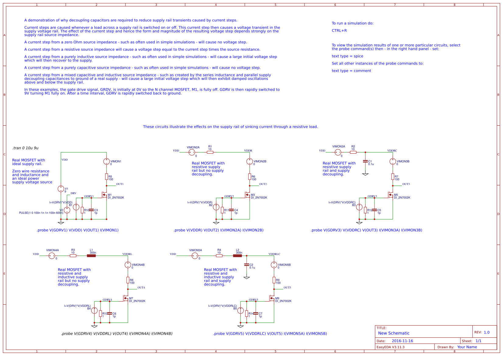
STD Power supply decoupling and why it matters.
License: Public Domain
Mode: Editors' pick
- 0
Update time:
2021-12-06 10:16:22
Creation time:
2016-11-16 11:55:31
Description
**This project is to demonstrate the need for and the basic effect of Power Supply Decoupling.**
In real circuits the power supply is not an ideal zero impedance source. The supply itself has some source resistance even though it may be in the order of tens of milliOhms. The wiring and PCB traces present a resistance but more importantly in terms of impedance, they present an inductance in series with the supply and some inherent parallel capacitance to ground.
If The supply comes from some sort of regulator it will have a load current transient response that may cause the output voltage to momentarily undershoot below and then overshoot above the nominal regulated output voltage. The behaviour of this under and overshoot is an indication of the stability of the regulator and is strongly dependent on the capacitance presented at the output of the regulator. For IC regulators, the recommendations in the device datasheet MUST be followed to ensure the stability of the regulator output voltage.
Even if the supply is from the output of a properly decoupled IC regulator, the wiring, leads and PCB traces both from the regulator output to the load and from the load back to ground, present additional resistance. More importantly however, in terms of impedance, they present an inductance in series with the supply and some inherent parallel capacitance to ground.
For example a 0.1mm diameter wire has an inductance of about 10nH/cm
(https://chemandy.com/calculators/round-wire-inductance-calculator.htm)
and a 0.2mm wide by 0.035mm thick (i.e. 1oz) copper PCB trace has an inductance of about 6nH/cm
(https://chemandy.com/calculators/flat-wire-inductor-calculator.htm).
Bearing in mind that the wiring length includes the path from and back to the supply it is easy to see how the inductance (Lser) in series with the supply can easily be in the region of 100nH.
The stray capacitance (Cpar) distributed between the supply and the load can also easily be in the region of a few tens to a couple of hundred pF.
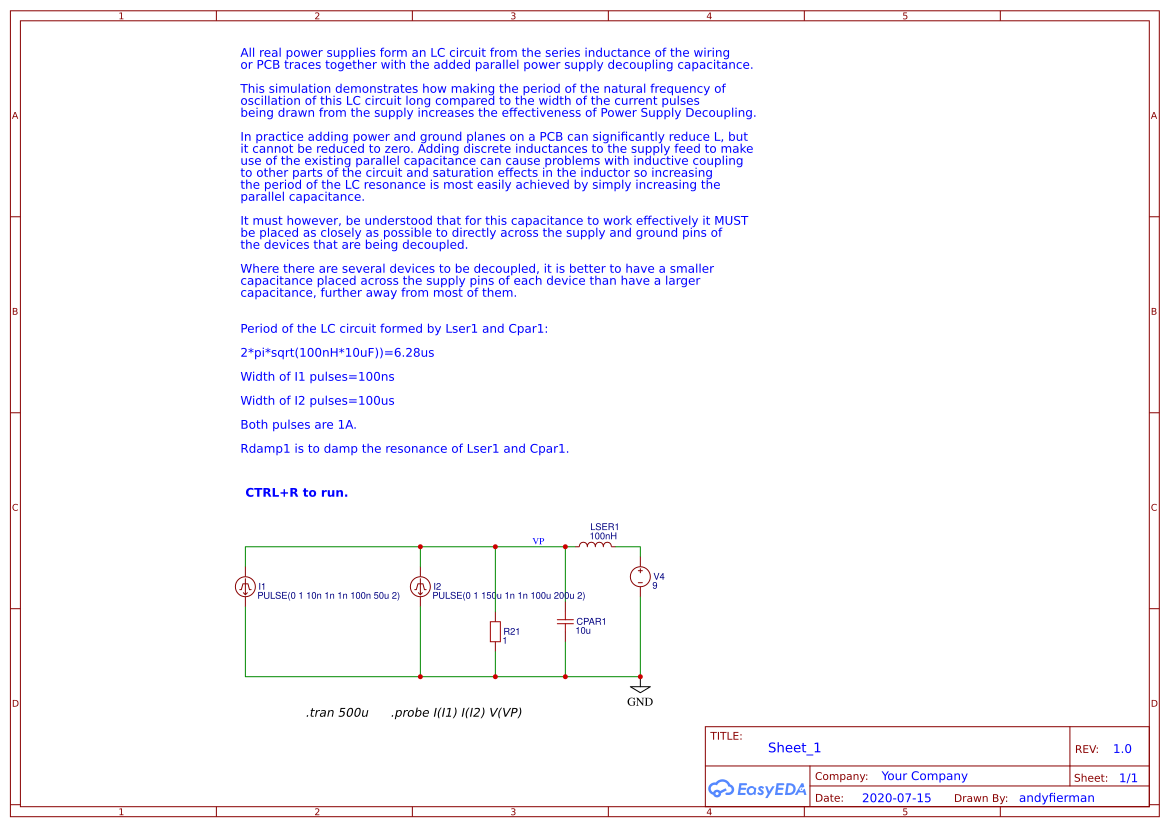
When a current step is drawn through a series inductance (Lser) with a parallel capacitance (Cpar) to ground, it will cause a large initial voltage drop which will then exhibit damped oscillations at the natural resonant frequency of the LC circuit above and below the supply rail. When the
current ceases there will be a large intitial voltage rise which will then exhibit damped oscillations below and above the supply rail. The closer together the current start and stop times are compared to the period of the natural resonant frequency of the LC circuit, the more the
response to the current start step tends to be cancelled out by the response caused by the current ceasing.
In other words if the period of the natural resonant frequency of the LC circuit formed by the series supply inductance and the parallel capacitance to ground is large compared to the time between the edges of the current steps or the width of the current spikes, the smaller the
overall voltage transient at the output of this LC circuit will tend to be.
The process of making the period of the natural resonant frequency of the LC circuit significantly lower than the time between the edges of the current spikes is called **Power Supply Decoupling**.
In real circuits it is not possible to make L or C zero and bearing in mind that in practical circuits every connection of a device to a supply creates its own little LC circuit local to that device, in practice it is usually easier to increase C by adding one or more physical
capacitors to the circuit local to each device, than it is to increase L by adding physical inductors in series with the supply to each device.
Decoupling across the supply pins is **essential** for all active devices such as op amps, comparators, amplifiers, voltage regulators, ADCs, DACs, gate drivers, timing and digital devices as well as across the supply and ground for discrete circuits that draw fluctuating supply currents such as transistor amplifiers, high and low side load switching circuits, motor and relay drivers.
In some cases such as low noise and RF circuits, a combination of series inductance and resistance with parallel caacitance to ground is added locally to each device but that is usually advised in the particular device datasheets and application notes and such additional decoupling measures are not generally required for most analogue and digital circuits.
This project includes simulations that demonstrate:
The basic effect of Power Supply Decoupling and the relationship between the period of the natural frequency of the LC circuit and the time interval between the edges of current steps.
Why decoupling capacitors are required to reduce supply rail transients caused by single ended load switching circuits such as transistor amplifiers and switches, relay and motor drivers;
Why decoupling capacitors are required to reduce supply rail transients caused by so-called shoot-through current spikes.
The additional effects of the same circuits driving a resistive load.
Why decoupling capacitors are **essential** when using bipolar technology versions of the 555 timer IC.
To run a simulation do:
`CTRL+R`
To view the simulation results of one or more particular circuits, select and
set the probe command(s) then - in the right hand panel - set:
`text type = spice`
Set all other instances of the probe commands to:
`text type = comment`
More background information here:
https://en.wikipedia.org/wiki/Decoupling_capacitor
Design Drawing
schematic diagram
(
1
/
)
-

An example of power supply decoupling in action
Open in Editor -

Another example of power supply decoupling in action
Open in Editor -

More examples of power supply decoupling in action
Open in Editor -

Decoupling 555 timer circuits
Open in Editor -

Short vs long current pulses
Open in Editor
PCB
(
1
/
)
The preview image was not generated, please save it again in the
editor.
| ID | Designator | Footprint | Quantity |
|---|---|---|---|
| 1 | B1 | NONE | 1 |
| 2 | B2 | NONE | 1 |
| 3 | B3 | NONE | 1 |
| 4 | B4 | NONE | 1 |
| 5 | B5 | NONE | 1 |
| 6 | C1,C2 | C0805 | 2 |
| 7 | C3,C4,C5,C6,C7 | C0805 | 5 |
| 8 | L1,L2 | INDUCTOR-1206 | 2 |
| 9 | M1,M3,M5,M7,M9 | NONE | 5 |
| 10 | M2,M4,M6,M8,M10 | SOT23 | 5 |
| 11 | R1,R2,R3,R4 | R0805 | 4 |
| 12 | R5,R6,R7,R8,R9 | R0805 | 5 |
| 13 | R10,R11,R12,R13,R14,R5,R6,R7,R8,R9 | R0805 | 10 |
| 14 | V1 | 2P-5.0 | 1 |
| 15 | V2 | 2P-5.0 | 1 |
| 16 | VIMON1,VIMON2A,VIMON2B,VIMON3A,VIMON3B,VIMON4A,VIMON4B,VIMON5A,VIMON5B | 2P-5.0 | 9 |
| 17 | V2 | 2P-5.0 | 1 |
| 18 | C8 | RAD-0.1 | 1 |
| 19 | C9 | RAD-0.1 | 1 |
| 20 | C10 | RAD-0.1 | 1 |
| 21 | L3 | AXIAL-0.4 | 1 |
| 22 | R15,R16,R19,R20 | AXIAL-0.3 | 4 |
| 23 | R17,R18 | AXIAL-0.3 | 2 |
| 24 | U1,U2 | DIP8 | 2 |
| 25 | V3,V4 | HDR1X2 | 2 |
| 26 | CPAR1 | RAD-0.1 | 1 |
| 27 | I1 | 2P-5.08 | 1 |
| 28 | I2 | 2P-5.08 | 1 |
| 29 | LSER1 | AXIAL-0.4 | 1 |
| 30 | R21 | AXIAL-0.3 | 1 |
Unfold
Project Members


 0
0
 0
0
Collect to album
Related Projects
Change a batch
Loading...
Add to album
×
Loading...
reminder
×
Do you need to add this project to the album?