


© 2024 EasyEDA Some rights reserved ISO/IEC
Editor Version
×
Standard

1.Easy to use and quick to get started
2.The process supports design scales of 300 devices or 1000 pads
3.Supports simple circuit simulation
4.For students, teachers, creators
Profession

1.Brand new interactions and interfaces
2.Smooth support for design sizes of over 5,000 devices or 10,000 pads
3.More rigorous design constraints, more standardized processes
4.For enterprises, more professional users
Ongoing
STD Welcome to EasyEDA
License: Public Domain
Mode: Editors' pick
- 13
Update time:
2021-03-18 10:23:27
Creation time:
2017-09-12 12:19:27
Description
These are some notes to help you create successful PCB projects and also have fun on the way.
Please note that it is strongly advised that you don’t start off by trying to create an actual project.
Start by reading this and the linked documents.
Then create a dummy project, the sole purpose of which is to play with the tools and learn how to use them. Learning through play is a powerful technique and is not just for kids!
1) To save a lot of pain and confusion later, please take the time to read the:
[EasyEDA Tutorial](https://docs.easyeda.com/en/Introduction/Introduction-to-EasyEDA/index.html)
* This will help you to learn to drive EasyEDA.
2) and then before you start your **Circuit Design** please read:
2.1) [From Idea to PCB: an EasyEDA Design Procedure](https://easyeda.com/andyfierman/From_Idea_to_PCB_an_EasyEDA_Design_Procedure-78173f41ed2d468cb6880e6d21483f11)
2.2) [How to design PCBs](https://docs.google.com/document/d/1CU7RuPyFlSZPzWBN-YZ0x87xeAB4xpLdLaIsUwhLj_M/edit?usp=sharing)
(I am in the process of writing this detailed tutorial on how to create a schematic and then do a PCB design. It is a work-in-progress and will eventually make it onto the EasyEDA site but it is useful as it is right now and you can see the current draft at the above url.)
* This will help you understand what you need to do to create a schematic and a PCB in EasyEDA with the minimum effort and the maximum chance of a successful outcome and why.
and:
2.3) [How to create findable footprints and searchable symbols](https://docs.google.com/document/d/1ZRkPPMID68mBz9j9RMIJARNSXK12PDULZXP7kiThvDg/edit?usp=sharing)
This will help you to find symbols and footprints and understand how to successfully create your own so that you and others can find them and be assured that they are correct.
3) If you wish to **Simulate** your design then you **must** also read the:
[Simulation Tutorial](https://docs.easyeda.com/en/Simulation/Headings/index.html)
4) Then before you start doing your **Schematic Capture**, please take the time to read:
[Essential checks before clicking the Convert Project to PCB, Update PCB or Import Changes buttons](https://easyeda.com/andyfierman/Essential_checks_before_clicking_the_Convert_Project_to_PCB_Update_PCB_or_Import_Changes_buttons_-7d2c6484b0c74aea930b1acf6459cd39)
* This will help you complete and check all the necessary steps to prepare a schematic that will successfully convert into a PCB.
5) Do your schematic capture and then before you click on the **Convert Project to PCB...** button in the schematic editor to start your **PCB Design** please *re-read the above link*.
6) Do your PCB Design and then before you click on the **Fabrication Output...** button in the PCB editor and submit your PCB Order please read:
[Essential checks before placing PCB order](https://easyeda.com/andyfierman/Essential_checks_before_placing_a_PCB_order-de51f1401cec4bd2896ea835aca67db8)
* This will help you complete and check all the necessary steps to prepare a PCB Design that will successfully convert into a PCB that is physically and electrically correct to the Schematic.
#### Note that none of these steps can help you design a circuit in the first place but if you start with a circuit design that works, they will significantly increase the chances that it will work when it is built on the PCB you have designed in EasyEDA.
:)
Design Drawing
schematic diagram
(
1
/
)
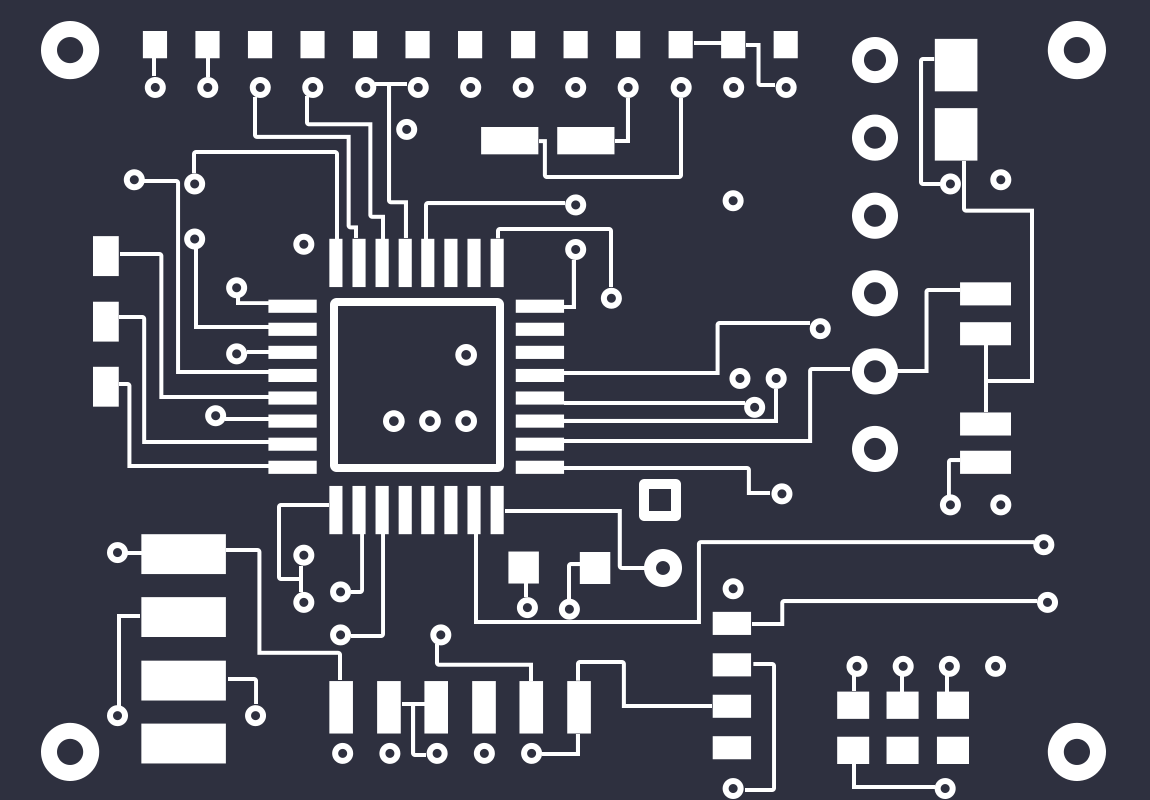
PCB
(
1
/
)
The preview image was not generated, please save it again in the
editor.
BOM
Project Members


 1
1
 13
13
Collect to album
Target complaint
Related Projects
Change a batch
Loading...
Add to album
×
Loading...
reminder
×
Do you need to add this project to the album?