


© 2024 EasyEDA Some rights reserved ISO/IEC
Editor Version
×
Standard

1.Easy to use and quick to get started
2.The process supports design scales of 300 devices or 1000 pads
3.Supports simple circuit simulation
4.For students, teachers, creators
Profession

1.Brand new interactions and interfaces
2.Smooth support for design sizes of over 5,000 devices or 10,000 pads
3.More rigorous design constraints, more standardized processes
4.For enterprises, more professional users
Ongoing
STD PCB Layout Software
Mode: Editors' pick
- 0
Update time:
2021-04-12 06:03:46
Creation time:
2015-11-30 13:52:00
Description
PCB Layout Software:
Our Easyeda software is a snap to learn and use .Laying out PCB is easy , even for the first time user .Here are some steps:
Step1:
Select the components: -Begin your layout by adding the components .Select the parts from the General Package .
Step2:
Position the components:-Drag each component to the desired location on the board .The snap feature makes it easily to align the parts .Draw the external mechanical framework of the PCB boards.
![enter image description here][1]
Step3:
Add the Traces :– Now add each trace by clicking on the pin of a component and dragging the trace to another pin.
![enter image description here][2]
Step4:
Edit the Layout:-Making changes is simple using standard commands such as Copy, Cut and Paste.Rearrange the parts by dragging them with the mouse.Traces always stay connected to their pins, even when you move things around. You can set the properties of items in your layout by double click them .For example , you can double click the traces to change its layer or width or you can double click the text to change the name of the components .
![enter image description here][3]
Step5:
Measure the Length and Heigth of the PCB Board —Mostly we need to measure exactly how long the width and the height of the PCB board . Easyeda provides an ICON named Dimension in the in the PCB Tools to messure the distance between two points . Click it to meassure the width and heigth of the PCB board . Most of the PCB boards need to be installed on mechanical structure, so you need to add the hole on the rim of the PCB board .
![enter image description here][4]
Step6:
Preview Gerber file : —After you complete PCB layout ,the easyeda provides you with the function of previewing the Gerber file .Check whether it is suitable for production .On the Gerber file , you could preview the Top Side of the PCB board, the bottom Side of the PCB board ,With Silk layer or not ,different colors of PCB board ,Silver Plating or Gold Plating .
![enter image description here][5]
![enter image description here][6]
Step7:
Order your PCBs:—The easyeda provides a function of ordering your PCBs .Click Fabrication Output and the PCB board will be Added to the Cart .Set the Layers ,PCB Dimension Width, PCB Dimension Height ,PCB Thickness, PCB Qty and so on . Then save to Cart , order PCB and wait for your PCBs.
![enter image description here][7]
![enter image description here][8]
![enter image description here][9]
![enter image description here][10]
![enter image description here][11]
![enter image description here][12]
[1]: /editor/20151121/565048de080f9.png
[2]: /editor/20151121/564fe6e5b345a.png
[3]: /editor/20151121/564fe6fee6151.png
[4]: /editor/20151121/565047f36ae95.png
[5]: /editor/20151121/56504aa4a64ef.png
[6]: /editor/20151121/5650480c9d098.png
[7]: /editor/20151121/5650481784b85.png
[8]: /editor/20160218/56c53c5cf0dbe.jpg
[9]: /editor/20160218/56c550485e93c.gif
[10]: /editor/20160218/56c55a648dee3.png
[11]: /editor/20160218/56c55ad0ef708.png
[12]: /editor/20160218/56c55ad9b3052.jpg
Design Drawing
schematic diagram
(
1
/
)
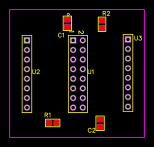
PCB
(
1
/
)
The preview image was not generated, please save it again in the
editor.
BOM
Project Members


 0
0
 0
0
Collect to album
Target complaint
Related Projects
Change a batch
Loading...
Add to album
×
Loading...
reminder
×
Do you need to add this project to the album?