


© 2024 EasyEDA Some rights reserved ISO/IEC
Editor Version
×
Standard

1.Easy to use and quick to get started
2.The process supports design scales of 300 devices or 1000 pads
3.Supports simple circuit simulation
4.For students, teachers, creators
Profession

1.Brand new interactions and interfaces
2.Smooth support for design sizes of over 5,000 devices or 10,000 pads
3.More rigorous design constraints, more standardized processes
4.For enterprises, more professional users
Ongoing
STD PCB Layout Tutorial
Mode: Editors' pick
- 8
Update time:
2021-04-12 06:03:46
Creation time:
2016-09-26 06:59:37
Description
In this **PCB layout tutorial** I hope to tell you how to create a good PCB layout very easily and clearly. I’d like to take [EasyEDA PCB design editor][1] as an example because it’s free, easy-to-use and without any installation but it brings you fast PCB design and easier circuit design experience.
**Step 1: Convert your schematic to a PCB**
First you could draw your schematic on [EasyEDA editor][2] as below image showed. I’m using this music controlled LED’s schematic for this tutorial:
![enter image description here][3]
Once you’re done with your schematic, you could click on “**Convert project to PCB**”
![enter image description here][4]
**Step 2: Placing the components**
Now it’s time to drag and drop the components to the spots where you want them to be.
If you want your PCB to look as clean as possible I suggest placing all components with the same function next to each other, like resistors for example.
Also make sure to leave some extra space between components, especially capacitors since the size may vary. Apart from the fact that the size may vary leaving some space will make the soldering a lot easier. Especially when you have to solder SMD components.
**Step 3: Drawing a custom outline**
First, select the “**BoardOutline**” layer in the **layers menu**:
![enter image description here][5]
Click on the current outline (the pink square in your editor) and press delete to get rid of it.
Now you can use the **PCB tools** to draw a new outline:
![enter image description here][6]
Once you’re done with your outline you can switch back to either the top or bottom layer.
**Step 4: Creating a copper area (GND)**
A very easy way to connect a lot of parts to a signal (mostly used GND) is to create a copper area.
You can create a copper area by using the tool “Copper Area” in the Tools menu.
Once you’re done drawing just outside of the outline your PCB should look something like this:
![enter image description here][7]
Now click on the dotted line you just drew and check whether these settings are correct. Once they are correct you can click “Rebuild CopperArea” and your PCB will be filled with copper only connecting to GND.
![enter image description here][8]
**Step 5: Routing**
There are 2 different ways to perform this step. The easiest is to use the “Auto Router” function. If you’re creating a PCB where the current is low you can use this method, but if you need different track sizes you’re better off routing the PCB yourself.
The **Auto Router** function can be found here:
![enter image description here][9]
You should see blue lines all over the PCB. These indicate which component’s pin is connected to which pin.
![enter image description here][10]
Now use the “Track” tool in the tools menu and click on a pad. Once you move your mouse you should see the blue line moving as well. Make sure not to cross any other tracks or pads and start routing all tracks to the correct pads.
You can switch to the opposite layer (top/bottom) if you have to cross lines.
If you have to switch to another layer for a SMD component you have to use a “via” which can also be found in the tools menu. A via is basically a copper connection between multiple layers.
This is an example of what your PCB could look like (With “Fill Style” None in the copper area properties):
![enter image description here][11]
**Step 6: Adding holes**
If you want to mount your PCB onto something it might be useful to add some holes.
Click on the “Hole” tool in the tools menu. Now you can set the size of the hole on the right.
**Make sure you’re using the right units!!**
Once the size has been set you can click on the spots you want your holes to be.
Don’t place holes onto components or tracks. Resize your PCB outline if you need more space to add the holes.
**Step 7: Adding Text and Images**
To add text click on the “Text” or “Image” tool in the tools menu. Place the text where you want it to be and change the text in the right properties menu.
You can also change the desired layer in the menu.
Step 8: Finalizing the PCB
You can take a look at the finished result by clicking on the **“Photo View”** button:
![enter image description here][12]
Once clicked you can find different options like top/bottom side, but also the color of the PCB.
Once you’re satisfied with the result you can click on **“Fabrication Output”** to buy the PCB’s using the service EasyEDA is also providing.
![enter image description here][13]
I hope this **PCB layout tutorial** has helped you improve your PCB designing skills. If you are interested in creating your PCB and learning how to manage EasyEDA PCB design editor, you could check this [video][14] and more step by step [tutorial][15].
[1]: https://easyeda.com
[2]: https://easyeda.com/editor
[3]: /editor/20160926/57e8ca1c99218.png
[4]: /editor/20160926/57e8c7f1e9103.png
[5]: /editor/20160926/57e8c8208f200.png
[6]: /editor/20160926/57e8c8394d2af.png
[7]: /editor/20160926/57e8c859dfdbe.png
[8]: /editor/20160926/57e8c86398917.png
[9]: /editor/20160926/57e8c88688459.png
[10]: /editor/20160926/57e8c89c21fca.png
[11]: /editor/20160926/57e8c8a5b0499.png
[12]: /editor/20160926/57e8c8ea3c49f.png
[13]: /editor/20160926/57e8c8f823880.png
[14]: https://www.youtube.com/watch?v=EoT2D2PLzVE
[15]: https://easyeda.com/Doc/Tutorial/
[16]: /editor/20160926/57e8c90018236.png
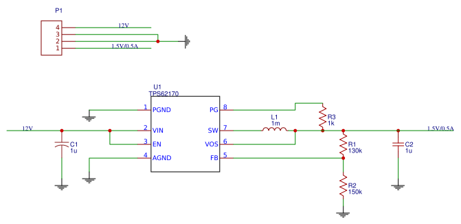
Design Drawing
schematic diagram
(
1
/
)
PCB
(
1
/
)
The preview image was not generated, please save it again in the
editor.
| ID | Name | Designator | Footprint | Quantity |
|---|---|---|---|---|
| 1 | TPS62170 | U1 | DIP | 1 |
| 2 | 1u | C1 | CP_8X13MM | 1 |
| 3 | 1m | L1 | INDUCTOR-1206 | 1 |
| 4 | 130k | R1 | R3 | 1 |
| 5 | 150k | R2 | R3 | 1 |
| 6 | 1u | C2 | C1 | 1 |
| 7 | 1k | R3 | R3 | 1 |
| 8 | SIP4 | P1 | HDR1X4 | 1 |
Unfold
Project Members


 0
0
 8
8
Collect to album
Target complaint
Related Projects
Change a batch
Loading...
Add to album
×
Loading...
reminder
×
Do you need to add this project to the album?