© 2024 EasyEDA Some rights reserved ISO/IEC
Editor Version
×
Standard


1.Easy to use and quick to get started
2.The process supports design scales of 300 devices or 1000 pads
3.Supports simple circuit simulation
4.For students, teachers, creators
Profession


1.Brand new interactions and interfaces
2.Smooth support for design sizes of over 5,000 devices or 10,000 pads
3.More rigorous design constraints, more standardized processes
4.For enterprises, more professional users
Ongoing
STD From Idea to PCB: an EasyEDA Design Procedure copy
License: Public Domain
Mode: Editors' pick
Cloned from From Idea to PCB: an EasyEDA Design Procedure
- 0
Update time:
2019-01-21 19:27:25
Creation time:
2019-01-21 19:27:25
Description
## Introduction
This post describes a Design Procedure to help take an idea for an electronics project through to PCB.
## Capture the design requirements
Once an initial idea has been formed, the first stage of any electronics project is to define what the circuit to be designed is required to do.
This is referred to as a **Design Requirements Specification**.
Without a Design Requirements Specification the design aims are undefined and therefore it is not possible to decide if any particular circuit will meet them.
Once a Design Requirements Specification has been created it is possible to compare the capabilities of any candidate circuit against these specifications and from there see which best meets the original requirements.
It is important to focus on - but also to keep an open mind about - the design task. There may be more than one way to achieve the design aims and often a better solution can be arrived at by considering the Pros and Cons of several possible solutions.
The existence of a Design Requirements Specification makes it possible to consider several different circuit implementations and to cherry pick the best bits of them to arrive at a good solution.
## Capture and develop the design
There are several ways to approach the design of each circuit implementation.
1) Copy an existing circuit, entering it into a Schematic Capture tool such as EasyEDA with the necessary supporting information to successfully turn it into a PCB;
2) Start with pencil and paper to draw the circuit starting with a sketch of a basic idea and then refine it towards a final circuit design with all necessary design calculations carried out using tools such as pencil and paper, calculator, spreadsheets, maths packages (e.g. Scilab, Scicos, Octave, SMath Studio etc.), device datasheets and applications notes. Then enter the final design into a Schematic Capture tool such as EasyEDA adding the necessary supporting information to successfully turn it into a PCB;
3) Start with a Schematic Capture tool such as EasyEDA to draw the circuit starting with a sketch of a basic idea and then refine it towards a final circuit design with all necessary design calculations carried out using tools such as pencil and paper, calculator, spreadsheets, maths packages (e.g. Scilab, Scicos, Octave, SMath Studio etc.), device datasheets and applications notes. The necessary supporting information to successfully turn the schematic into a PCB must be added as the schematic is developed;
4) Start with a Schematic Capture and Simulation tool such as EasyEDA to draw, model and simulate the circuit starting with a sketch of a basic idea and then refine it towards a final circuit design supported by the simulations and other design calculations primarily carried out using the simulation tool itself as well as other tools such as pencil and paper, calculator, spreadsheets, Maths packages (such as Scilab, Scicos, Octave, SMath Studio etc.), device datasheets and applications notes. The necessary supporting information to successfully turn the schematic into a PCB must be added as the schematic is developed
Of these options, clearly (1) is the least effort but is only viable if a suitable circuit is already available.
As soon as any variation to an existing circuit is required or a new circuit is to be designed then approaches (2), (3) or (4) must be used.
With the availability of tools such as EasyEDA. approach (2) is effectively superseded by approaches (3) and (4).
## Why simulate?
Accepting that it may not always be necessary, practical or even possible to simulate a circuit, for those that *can* be modelled and simulated to some useful extent there are significant benefits in adopting approach (4).
In applications where it may not be necessary, practical or even possible to simulate the whole circuit, it can still be very helpful in understanding the basic operation of - or the operational limits on - a circuit by modelling and simulating the most important parts of it.
By starting a design in simulation and using the Schematic Capture and Simulation tools like a sketchpad, different ideas can be quickly tried out and tested. The most promising parts of each possible solution can then be cherry picked (i.e. copied and pasted) and a final design converged upon quickly and cheaply because there is little or no reliance on building breadboards or even prototypes.
A second benefit of simulation is that the internal signal conditions of components can be probed by observing their operation in the simulation. This can often be hard to do in a real circuit without the probing adversely affecting the operation of the circuit.
For example, this can be very helpful in checking that the currents in inductors and that the ripple currents in capacitors are staying within their specified limits. Another example is probing voltages on very high impedance nodes such as on the gates of MOSFETs used in capacitive sensors. Such currents and voltages may be hard to probe in a real circuit without some quite expensive test equipment. Simply being able to probe a simulation can be helpful is understanding why one circuit may be better than another or why a circuit does not behave as expected or simply does not work.
A third benefit is that it is possible to test a simulation to destruction such as during worst case, fault and failure mode analysis without actually doing any damage to what may be - in a real circuit - costly components.
A fourth benefit of simulation is that it is also immensely useful in the debugging stages of working on a design once it has been built on a PCB. By comparing measurements of the real circuit with those made in the simulation it is often possible to infer what may be causing the real circuit to operate in some unexpected way. By introducing to the simulation, parasitics such as capacitances or inductances to represent those that may have been created by the real PCB layout but which were not known at the time of and hence could not be included in the original simulation, it may be possible to then modify the simulation so that its behaviour is more like that of the real circuit. This can then give verifiable insights into what is actually the cause of the difference between the desired and the actual circuit behaviour.
A fifth significant benefit of simulation is that for the parts of a circuit that can be simulated, the connectivity of that circuit can be verified by observing the circuit operation in the simulation. As will be explained below, this can save a lot of time and effort in creating the schematic that will ultimately be used to create the PCB.
## The 'Traditional' route to PCB
The traditional route to creating a PCB is to start by creating a Schematic for the circuit to be built on the PCB.
This schematic contains all the components that are to be mounted on or form an integral part of the PCB. The symbols in this schematic are simply graphical representations of the components together with information about their PCB package type, pin mappings, manufacturers, suppliers and associated part numbers and a brief description.
* These symbols are referred to as **Schematic Symbols**.
Schematic Symbols are used in the schematic simply to show how the components are connected. In other words they are just a graphical representation of a netlist describing the connectivity of the circuit.
Except for the basic passive components (resistors, capacitors and inductors), Schematic Symbols do not have simulation models associated with them. Hence a schematic created using this type of symbol can convey no information about how the circuit actually functions or behaves.
* Most of the symbols in the EasyEDA Library are Schematic Symbols.
* A schematic created purely for the purposes of producing a PCB and built using Schematic Symbols, can therefore be referred to as a **Non-Simulation (or Passive) Schematic**
* The Project containing this Non-Simulation Schematic and the PCB designed from it can therefore be referred to as a **Non-Simulation (or Passive) Project**.
## Some problems with the 'Traditional' route to a PCB.
This traditional approach builds a schematic that is ready to be passed into PCB layout.
It is often only at this point that any thought is given to simulating the design to see if it works.
This is, in the author's opinion, entirely the wrong time to embark on simulation work.
It is the tail wagging the dog.
There are several problems with doing simulation at this late stage.
One is that a schematic created for PCB layout is almost certainly not directly suitable for simulation. It will have extra components such as connectors, mechanical switches and fuses which may have little bearing on the outcome of a simulation but which will eat up simulation resources. It will often lack input signal and power supply sources and output loads that will be required in the simulation. The symbols used in the schematic may well have been chosen with no consideration of their having spice models associated with them.
Therefore a lot of work is required to prepare a copy of the Non-Simulation Schematic for simulation. In preparing the Non-Simulation Schematic for simulation there is an inevitable risk of introducing mistakes into the connectivity of what had been a checked and known to be correct schematic.
The second problem is that in trying to simulate a schematic of a whole circuit even after it has been prepared for simulation, for a number of reasons, it is quite likely to fail on its first run. It is then very difficult to debug. It is much better to simulate circuits in smaller sections and build up to the full circit from these tested smaller sections.
A third problem is that if any changes are required as a result of the simulation, it may be that the PCB is already in layout then extra work will be needed to update the PCB in response to the changes needed in the schematic.
Essentially, it is all too easy for the original schematic and the one prepared for simulation to diverge. This then renders the purpose of simulation somewhat debatable and also raises the question of which version of the circuit is the correct one.
## A better route to a PCB.
An alternative route to creating a PCB which avoids most of these pitfalls is to start with a simulation of the circuit, working from initial ideas and circuit 'sketches', building up to a full circuit as described in approach (4) above.
* Not surprisingly a Project containing a schematic created for the purposes of simulating all or parts of the circuit can therefore be referred to as a **Simulation (or Active) Project**.
The objective of a Simulation Project is to try to prove that a design works by simulating it.
Simulating a design is also a good way of proving that the components in the circuit are connected correctly. In other words that the connectivity of the circuit (i.e. the netlist) is correct.
* A circuit is simulated by creating a **Simulation (or Active) Schematic**.
The difference between a Simulation Schematic and a Non-Simulation Schematic is that the symbols used in a Simulation Schematic have simulation models associated with them.
* The symbols used in a Simulation Schematic are referred to as **Spice Symbols**.
A Spice Symbol for a given device can look identical to a Schematic Symbol for the same device and the only way to distiguish them in the library is by which part of the library they come from (**System Components > Spice Simulation**) and by the small `s` in the symbol icon in the `Title (PartNO)` column of the SHIFT+F results list.
### Identifying a Schematic Symbol
![enter image description here][1]
### Identifying a Spice Symbol
![enter image description here][2]
Although it is not possible to create a PCB directly from a Simulation Schematic, all the information needed to do so (PCB package type, pin mappings, manufacturers, suppliers and associated part numbers and a brief description) can be put into the Spice Symbol in the same way as for a Schematic Symbol. If this is done, these symbols can then be used in the creation of a PCB as described below.
The Simulation Schematic contains most but not all of the components that will go into the Non-Simulation Schematic that will then be used to create the PCB. For example the simulation schematic for an audio amplifier will usually contain all of the active components such as transistors and operational amplifiers but may omit things like voltage regulators, decoupling capacitors, connectors, logos and warning labels and possibly fuses or fuse holders.
However, in the same way that a real circuit needs a power source, a signal source and perhaps control signals, some form of power supply and signal or control source is needed in the Simulation Schematic.
Regulators and other supply rails are usually replaced with idealised voltage sources. Using ideal sources there is then no point in including decoupling capacitors because they have no effect on the simulation.
Unless it is particularly required to simulate their effects for Signal or Power Integrity or RF work, connectors are usually omitted with components simply connected directly by idealised zero impedance `wires` (nets and netlabels).
Switches and relays - particularly mechanical ones - may be replaced in the simulation by simplified models ranging from simple fixed resistances through voltage or current controlled switches or other more complex behavioural models. Solid state switches and in some cases MOSFETs used as switches may be replaced by suitable device symbols but which have simplified behavioural models associated with them.
A Non-Simulation schematic for this amplifier would not contain the loudspeaker but for a Simulation Schematic, a load representing this loudspeaker would usually be required. So even though things like loudspeakers or motors which may not be on the PCB and so would not be in a Non-Simulation Schematic, they will be required as part of the Simulation Schematic.
In a Simulation Schematic, power and signal sources and output loads can be referred to as **Simulation Only** or **Simulation Support** elements and it is important to understand that these elements are only there to make the simulation work and therefore are not physical components that would appear in a Non-Simulation Schematic or a BoM of the same circuit for PCB Design.
* This means that a Simulation Schematic can be split into two sections: one comprising one or more sheets containing the circuit to be simulated and the other comprising one or more sheets containing only the Simulation Support elements.
* These two sections can be referred to as the **Simulation Schematic sheets** and the **Simulation Support Sheets** respectively.
In some designs, simulation may only be required - or perhaps is only possible - for part of a circuit.
It may be that a simulation - especially of a complicated circuit - may be best approached by breaking it up into smaller blocks where the output of one block may be modelled as a simplified or idealised source which can then be used as the input to the simulation of the next downstream block.
It is important to note that although it is possible to run a simulation in EasyEDA that is split into more than one sheet using:
**Super Menu > Miscellaneous > Netlist for Project**
it is not possible to choose which sheets are included in the simulation: EasyEDA will run all the sheets in the Project.
* Therefore if a simulation is split into more than one block (each comprising one or more Simulation Schematic sheets and one or more Simulation Support Sheets), each each simulatable block must be saved as a separate Simulation Project.
**Remember when doing this, that all nets and nodes with the same net name are connected together** so care must be taken to maintain the consistency of net names and netlabels across all the sheets in a Project.
Although there is no connectivity in EasyEDA between sheets saved in different Projects, as will be described later, it is also important to ensure that the net naming is consistent across all the different blocks
As an example of splitting a circuit into separate blocks, a pre-amplifier stage may be modelled and simulated in detail but when simulating the following power amplifier stage the output of the pre-amplifier stage may be modelled simply by an ideal voltage source.
In this case there would be a Pre-amplifier Simulation Project and a Power Amplifier Simulation Project.
Another example is where a voltage regulator circuit used to power the pre-amplifier stage is modelled in detail but the load presented to it by the pre-amplifier stage itself is simply modelled as a resistor with some capacitance (representing the decoupling in the pre-amplifier stage) in parallel with it.
In this case there would be a Voltage Regulator Simulation Project, a Pre-amplifier Simulation Project and a Power Amplifier Simulation Project.
* Breaking a simulation into separate Projects in this way can result in a whole set of Simulation Schematics (saved in a number of Simulation Projects), each of which, individually will not include everything that will be required in the final Non-Simulation Schematic but which when only the Simulation Schematic Sheets are taken overall (i.e. the Simulation Support Sheets are omitted) can still represent the core of the final Non-Simulation Schematic from which the PCB will be generated.
Simulation is an iterative task so there may be several passes through the Simulation Projects before a satisfactory set of Simulation Schematics is arrived at. The circuit, the Spice Symbols in it and/or their associated models may have to be changed but eventually a final set of schematics will be decided upon and the simulation work can be considered complete.
* Once the simulation work for a circuit has been completed, creating the Non-Simulation Schematic from a blank sheet wastes a great deal of time and runs a significant risk of introducing mistakes in the connectivity that have just been removed in the Simulation Schematic(s) as part of the simulation process. If the steps above are followed then it is also completely unnecessary.
## From Simulation Schematics to Non-Simulation Schematic
The steps to create the core of the new Non-Simulation Schematic are:
1) create a new (Non-Simulation) Project;
2) clone *only* the Simulation Schematic Sheets from the Simulation Project(s) into the new Non-Simulation Project (do not clone any of the Simulation Support Sheets);
3) check that net names are correct and consistent between separate schematic sheets;
The steps to complete the creation of the Non-Simulation Schematic suitable for passing into PCB Design are then:
4) insert into the Non-Simulation Schematic Sheets all the elements that were omitted from the Simulation Schematic(s) which were not required for the simulation but which are required to be on or form an integral part of the PCB. These will be components such as voltage regulator circuits, decoupling components, connectors, logos and warning labels and possibly fuses or fuse holders and any other components that it was not possible to simulate;
5) check and if necessary edit the net names and labels to maintain the correct connectivity after allowing for the insertion of these missing elements.
This approach still means that there are two different sets of schematics for simulation and for PCB but there is, in the author's opinion, less work and less chance of mistakes in the transfer of the simulation schematic into the Non-Simulation schematic than the traditional approach described above.
Below is a very simple example of a Simulation Project that is split into a Simulation Schematic Sheet and a Simulation Support Sheet:
https://easyeda.com/guest/Project_for_EDN_Simulation_schematic-eg93lfxPJ
Followed by the same circuit converted into a Non-Simulation Project:
https://easyeda.com/example/Project_for_EDN_Schematic_and_PCB-FHBvVPJ0i
## From Non-Simulation Schematic to PCB
Once the Non-Simulation Schematic has been created then the procedures described in:
https://easyeda.com/andyfierman/Essential_checks_before_clicking_the_Convert_Project_to_PCB_Update_PCB_or_Import_Changes_buttons_-7d2c6484b0c74aea930b1acf6459cd39
and:
https://easyeda.com/andyfierman/Essential_checks_before_placing_a_PCB_order-de51f1401cec4bd2896ea835aca67db8
should be followed to ensure a successful PCB design.
[1]: /editor/20171031/59f768e96bb93.png
[2]: /editor/20171031/59f7694009b9d.png
Design Drawing
schematic diagram
(
1
/
)
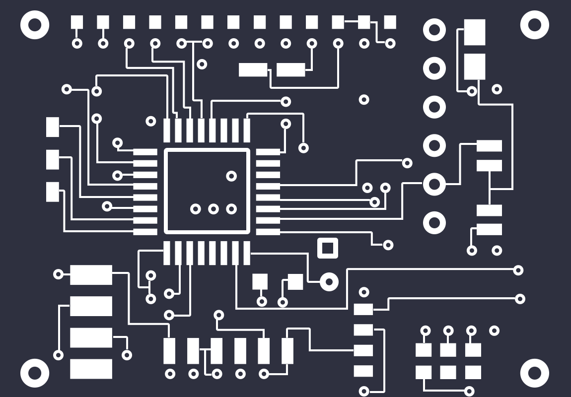
PCB
(
1
/
)
The preview image was not generated, please save it again in the
editor.
BOM
Project Members
Related Projects
Change a batch
Loading...
Add to album
×
Loading...
reminder
×
Do you need to add this project to the album?


