


© 2024 EasyEDA Some rights reserved ISO/IEC
Editor Version
×
Standard

1.Easy to use and quick to get started
2.The process supports design scales of 300 devices or 1000 pads
3.Supports simple circuit simulation
4.For students, teachers, creators
Profession

1.Brand new interactions and interfaces
2.Smooth support for design sizes of over 5,000 devices or 10,000 pads
3.More rigorous design constraints, more standardized processes
4.For enterprises, more professional users
Ongoing
STD Block for Intel® Edison - GPIO (Open hardware)
Mode: Editors' pick
- 0
Update time:
2021-04-11 16:39:59
Creation time:
2015-12-22 02:38:10
Description
Description: The Intel® Edison is an ultra small computing platform that will change the way you look at embedded electronics. Each Edison is packed with a huge amount of tech goodies into a tiny package while still providing the same robust strength of your go-to single board computer. Powered by the Intel® Atom™ SoC dual-core CPU and including an integrated WiFi, Bluetooth LE, and a 70-pin connector to attach a veritable slew of shield-like “Blocks” which can be stacked on top of each other. It’s no wonder how this little guy is lowering the barrier of entry on the world of electronics!
The GPIO Block is a simple breakout board to bring the GPIO from the Intel® Edison to the user. Bread board friendly, the GPIO Block provides access to all basic GPIO, PWM, and UART2 pins. All GPIO is level shifted to a selectable 3.3v or VSYS. The GPIO add-on also provides access to all three power rails found on the Intel® Edison. 3.3v, 1.8v, VSYS, and GND are accessible for bread board prototyping. Note: Since the level shifting is accomplished through a auto direction sensing translator, driving high current components (Such as Relays, Motors, and high power LED’s) will require an external switch. See the Hookup Guide to learn more.
[GitHub][1] (Design Files)
Sparkfun link:https://www.sparkfun.com/products/13038
![enter image description here][2]
[1]: https://github.com/sparkfun/Edison_GPIO_Block
[2]: /editor/20151231/5684e75904fc5.png
Design Drawing
schematic diagram
(
1
/
)
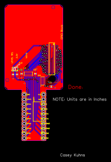
PCB
(
1
/
)
The preview image was not generated, please save it again in the
editor.
| ID | Name | Designator | Footprint | Quantity |
|---|---|---|---|---|
| 1 | FRAME-LETTER | FRAME1,FRAME2 | CREATIVE_COMMONS | 2 |
| 2 | OSHW-LOGO | LOGO1 | OSHW-LOGO-S | 1 |
| 3 | SFE_LOGO_NAME_FLAME | LOGO4 | SFE_LOGO_NAME_FLAME_.1 | 1 |
| 4 | FIDUCIAL | FID1,FID2,FID3,FID4 | FIDUCIAL-1X2 | 4 |
| 5 | M10 | JP1,JP2 | 1X10 | 2 |
| 6 | TXB0108 | U1,U4 | UFDFN-20 | 2 |
| 7 | 0.1uF | C1,C2,C3,C4,C5 | 0603-CAP | 5 |
| 8 | GPIO Reference Select | SJ1 | PAD-JUMPER-3-2OF3_NC_BY_PASTE_YES_SILK_FULL_BOX | 1 |
| 9 | EDISON_CONNECTOR_FULL | U2 | EDISON_DAUGHTER | 1 |
| 10 | EDISON_CONNECTOR_FULLHEADER | U3 | DF40C-70DP-0.4(51) | 1 |
Unfold
Project Members


 0
0
 0
0
Collect to album
Target complaint
Related Projects
Change a batch
Loading...
Add to album
×
Loading...
reminder
×
Do you need to add this project to the album?