


© 2024 EasyEDA Some rights reserved ISO/IEC
Editor Version
×
Standard

1.Easy to use and quick to get started
2.The process supports design scales of 300 devices or 1000 pads
3.Supports simple circuit simulation
4.For students, teachers, creators
Profession

1.Brand new interactions and interfaces
2.Smooth support for design sizes of over 5,000 devices or 10,000 pads
3.More rigorous design constraints, more standardized processes
4.For enterprises, more professional users

Ongoing
STD What is Multilayer PCB
License: Public Domain
Mode: Editors' pick
- 0
Update time:
2018-05-18 06:25:00
Creation time:
2018-05-18 05:35:37
Description
[Multilayer PCB](https://www.theengineeringprojects.com/2018/03/multilayer-pcb.html) is an integral part of most of the electronics when it comes to connecting number of electronic components on the board. [Multilayer PCB](https://jlcpcb.com) helps us getting rid of the old ways of joining components where components were joined together by end to end wiring, resulted in covering more space and weight and unable to fulfill the requirements of more complex designs.
Experts are in constant struggle to improve electronic design with compact shape so it provides better user experience and turns out to be less costly than its predecessors.
Now, you have got a clear idea why do we need PCB. There are already [different types of PCB board](https://www.theengineeringprojects.com/2018/03/different-types-of-pcb-printed-circuit-board.html) available in the market i.e. single layer board and double layer board. But, sometimes these boards fail to deliver more complex designs because of availability of less number of conductive layers on the board. Technology is evolving with the greater need of making devices cheap and low weight so they can meet the requirements in less cost and capable of performing more functions than using conventional ways of making electronic devices. [JLCPCB](JLCPCB) is one of PCB suppliers for single, double or multiple layers PCB at extremely low prices: $16 for 10pcs 4-layer PCB and $2 for 10pcs 2-layer PCB.
language
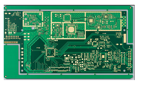
Multilayer PCB boards came into play with the intention of constructing more number of conductive layers on the board than single layer or double layer boards. Multi-layer boards come with a combination of single layer or double layer board and give opportunity to connect more electronic components in less space. These boards are made with number of conductive layers with insulated material between them.
Multilayer boards are mostly developed in rigid form, because making multilayer board in flexible form is very difficult to achieve and it also results in more cost than rigid boards. Instead of using flexible multilayer boards, most of the professionals prefer using combinations of single or double sided board that are very effective in most of cases and are cheaper than multilayer flexible boards.
Development of multilayer board totally depends on customers’ demands. With the invention of new technology multilayer boards can be manufactured with up to 100 conductive layers, making complex design where more number of components are joined together.
Smartphones are a great example of multilayer PCB that gives a benefit of performing more functions using single board. This refrains from spending more money on the combination of single sided or double sided boards, because they cost heavily with no guarantee of fulfilling requirements as multilayer PCB.

Multilayer boards can be manufactured with even conductive layers or odd conductive layers on them. However, it is recommended to use multilayer PCB with even layers because it results in simple design and helps in joining number of different components on the board where board design with odd layers can be costly and pertains to complex design, making it difficult to join number of electronic components on the board. Also, design with odd layers makes it very difficult twisting the board during execution of project, as odd layers are not equally distributed over the whole board structure which can damage the boards when they are subject to under heavy weights.
Some multilayer boards are manufactured so closely, making it very difficult of you to count the total number of layers with naked eye. However, still you can guess total number of layers based on the layers pattern and how they are laminated on the board.
Number of different conductive layers on the multilayer boards can be termed as signal, power or ground planes. Power or ground planes are directly proportional to the number of voltage requirements on the board, if there is a need of more than voltage supply on the board, then multilayer boards come with more than one power or ground planes.

Construction of multilayer board is little bit different than single layer or double layer boards as it exhibits more complex design with possibility of more complex functions. Multilayer boards are formed when prepreg and core material joined together under high temperature and pressure, helps in removing any trapped air between the layers. Prepreg used in multilayer board is more flexible and malleable than core material itself. After subjecting to high temperature and pressure, these material are then given some time to cool off, resulting in a hard, solid multilayer board where different conductive are equally distributed over the board.
Multilayer boards are widely used in most complex applications including cell phones, monitors, computers, signal transmission and many more. Main purpose of these boards is providing the pathway to perform complex functions over a single board without spending too much on the combination of different single layer or [2 layer PCB](https://jlcpcb.com). More great articles about PCB and electronic projects can be found on https://www.theengineeringprojects.com
Design Drawing
schematic diagram
(
1
/
)
PCB
(
1
/
)
The preview image was not generated, please save it again in the
editor.
BOM
Project Members


 0
0
 0
0
Collect to album
Target complaint
Related Projects
Change a batch
Loading...
Add to album
×
Loading...
reminder
×
Do you need to add this project to the album?