


© 2024 EasyEDA Some rights reserved ISO/IEC
Editor Version
×
Standard

1.Easy to use and quick to get started
2.The process supports design scales of 300 devices or 1000 pads
3.Supports simple circuit simulation
4.For students, teachers, creators
Profession

1.Brand new interactions and interfaces
2.Smooth support for design sizes of over 5,000 devices or 10,000 pads
3.More rigorous design constraints, more standardized processes
4.For enterprises, more professional users

Ongoing
STD ESQUEMA PARA IMPRIMIR EN PLACA
Mode: Editors' pick
- 0
Update time:
2021-08-13 15:48:17
Creation time:
2018-05-05 18:14:12
Description
Este esquema es el que se utilizara con los componentes correspondientes para la impresión de la placa y sera el que se utilizara de igual manera para el proyecto final
Design Drawing
schematic diagram
(
1
/
)
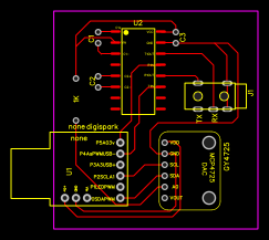
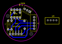
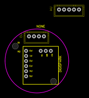
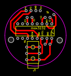
PCB
(
1
/
)
-

NEW_PCB
Open in Editor -

PCB1
Open in Editor -

PCB2
Open in Editor -

PCB3
Open in Editor -

NEW_PCB
Open in Editor
The preview image was not generated, please save it again in the
editor.
| ID | Name | Designator | Footprint | Quantity |
|---|---|---|---|---|
| 1 | LM358NG | A | OPAMP | 1 |
| 2 | 0.1UF | C1,C2,C3 | CAP-CBB-10.0*4.5 | 3 |
| 3 | gy4527 | GY4725 | MCP4725 | 1 |
| 4 | Straight headphone jack | J1 | AUDIO-PJ313D | 1 |
| 5 | Digispark_mat | U1 | DIGISPARK | 1 |
| 6 | ICL3232CBZ | U2 | MATRIX_3232 | 1 |
| 7 | RESISTOR | U3,U6 | RESISTOR | 2 |
| 8 | RESISTOR | U5 | OPA4134 | 1 |
Unfold
Project Members


 0
0
 0
0
Collect to album
Related Projects
Change a batch
Loading...
Add to album
×
Loading...
reminder
×
Do you need to add this project to the album?