


© 2024 EasyEDA Some rights reserved ISO/IEC
Editor Version
×
Standard

1.Easy to use and quick to get started
2.The process supports design scales of 300 devices or 1000 pads
3.Supports simple circuit simulation
4.For students, teachers, creators
Profession

1.Brand new interactions and interfaces
2.Smooth support for design sizes of over 5,000 devices or 10,000 pads
3.More rigorous design constraints, more standardized processes
4.For enterprises, more professional users

Ongoing
STD Acorn BBC Master Compact 128K system ROM
License: MIT License
Mode: Editors' pick
- 1
Update time:
2024-03-27 14:43:07
Creation time:
2023-08-01 09:15:29
Description
# Acorn BBC Master Compact 128K system ROM
In the Acorn BBC Master Compact MOS ROM *IC49* is by default a 64Kbyte ROM/27512 ROM chip, but if putting the jumper *PL12* on the *south* position a 128Kbyte chip can be put there.
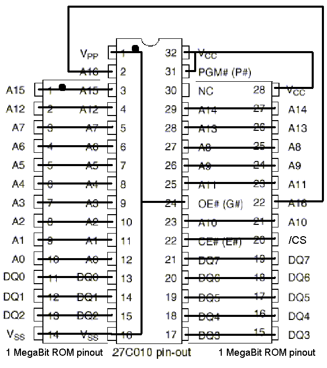
This is a DIP28 adaptor PCB to place two 27512 EEPROMs instead of a single 27C010.
## The system ROM socket *IC49*
Unfortunately the 128Kbyte/1Mbyte chip (27C010) is a DIP32 IC, but the socket on the Master Compact is a DIP28 one. I couldn't find any 1Mbyte parallel EPROM chip that fits on a DIP28 socket, so I guess that at Acorn they probably had in mind to use a mask ROM.
It is possible to build a dip 28 to dip 32 adapter to fit a 27C010 EPROM in the *IC49* system ROM socket.
Only 7 ROM space banks (9 to F) are assigned to the *IC49* ROM despite the 27512 EPROM can contain up to 4 16Kbyte ROM images because the MOS ROM isn't showed as bank 10. Only bank switchable ROMs are shown by the **ROM* command.
```
> *ROMS
ROM F UTILS 10 <----------- IC49 socket
ROM E BASIC 40 <----------- IC49 socket
ROM D ACORN ADFS 10 <------ IC49 socket
ROM C ? <------------------ IC49 socket with PL12 on south
ROM B ? <------------------ IC49 socket with PL12 on south
ROM A ? <------------------ IC49 socket with PL12 on south
ROM 9 ? <------------------ IC49 socket with PL12 on south
ROM 8 ?
RAM 7 ?
RAM 6 ?
RAM 5 ?
RAM 4 ?
ROM 3 ?
ROM 2 ?
ROM 1 ?
ROM 0 ?
```
### *PL12* jumper behaviour explanation
The MOS ROM is always selected (*CS* pin set *low*) and has the *OE* pin set to *low* if *PL12* is on the *north* position and a 27512 ROM chip is present. Otherwise what should have been a 20C1024 chip(?) will not have an *OE* pin and in place of it there will be the *A16* pin with *PL12* set on the *south* position.
## How to program the system and non-system ROMs for this PCB design
The system ROM must contain the `MOS` ROM in its top partition `0x00000000-0x00003FFF` and the non-system ROM must contain `DFS/ADFS`, `BASIC` and `UTILS` ROMs in this exact order in its bottom three paritions respectively in `0x00004000-0x00007FFF`, `0x00008000-0x0000BFFF` and `0x0000C000-0x0000FFFF`.
More specifically: \
For the system ROM
```
0x00000000-0x00003FFF corresponds to no ROM slot and must contain MOS
0x00004000-0x00007FFF corresponds to ROM 9
0x00008000-0x0000BFFF corresponds to ROM A
0x0000C000-0x0000FFFF corresponds to ROM B
```
For the non-system ROM
```
0x00000000-0x00003FFF corresponds to ROM C
0x00004000-0x00007FFF corresponds to ROM D and must contain DFS/ADFS
0x00008000-0x0000BFFF corresponds to ROM E and must contain BASIC
0x0000C000-0x0000FFFF corresponds to ROM F and must contain UTILS
```
The `*ROMS` command will not list the `MOS` ROM and will list the remaining ones starting from the one at the bottom of the memory from the non-system ROM listed as `ROM F`, through the one at the top of the system ROM listed as `ROM 9`. \
This memory layout is basically the same that we would have had if we were using a `27C010` EPROM because the two `27512` are "emulating" a single `27C010`. \
The system will not boot at all if at least the `MOS` and `UTILS` ROMs aren't palced at the right places.
## ROM ICs
| ROM IC socket | EPROM | space bank | size | description |
| --- | --- | --- | --- | --- |
| IC49 | 27512 or 27C010 | D to F or 9 to F | 64Kbyte or 128Kbyte | system ROM quadruple or octuple image ROM |
| IC29 | 27128 | 8 | 16Kbyte | single image ROM |
| IC38 | 27128 or 27256 | 1 or 0 to 1 | 16Kbyte or 32Kbyte | edge connector or internal double image ROM |
| IC23 | 27128 | 2 | 16Kbyte | single image ROM |
| IC17 | 27128 | 3 | 16Kbyte | single image ROM |
## GitHub tool to merge multple ROM images into a single file
The following GitHub project can be used to merge 4 ROM images into a single one that can be programmed into a single 27128 EPROM chip
[github.com - ROM_images_merger](https://github.com/DanCasterIt/ROM_images_merger)
A Windows x86 (32-bit) executable file is pushed into the repository so that the program can be runt without compiling it.
Usage example to generate the ROM images for the system and non-system ROMs ready to be programmed:
```
$ ./ROM_image_generator Internet_pc128s_rom/OS51.ROM KERMROM basiced EDITROM
Input the memory size in bytes. (0 for 65536): 0
Input the number of equally sized partitions. (0 for 4): 0
Input if to fill blank partitions with ones (1) or zeros (0): 0
Found 4 files. Choose where to place them.
partition 0 @ 0x00000000-0x00003FFF filled with file: Internet_pc128s_rom/OS51.ROM
partition 1 @ 0x00004000-0x00007FFF filled with file: KERMROM
partition 2 @ 0x00008000-0x0000BFFF filled with file: basiced
partition 3 @ 0x0000C000-0x0000FFFF filled with file: EDITROM
Apply changes? (y or n): y
Writing "ROM_image.bin"...
$ mv ROM_image.bin ROM_imageA.bin
$ ./ROM_image_generator DFSimage Internet_pc128s_rom/ADFS210.ROM Internet_pc128s_rom/BASIC48.ROM Internet_pc128s_rom/UTILS.ROM
Input the memory size in bytes. (0 for 65536): 0
Input the number of equally sized partitions. (0 for 4): 0
Input if to fill blank partitions with ones (1) or zeros (0): 0
Found 4 files. Choose where to place them.
partition 0 @ 0x00000000-0x00003FFF filled with file: DFSimage
partition 1 @ 0x00004000-0x00007FFF filled with file: Internet_pc128s_rom/ADFS210.ROM
partition 2 @ 0x00008000-0x0000BFFF filled with file: Internet_pc128s_rom/BASIC48.ROM
partition 3 @ 0x0000C000-0x0000FFFF filled with file: Internet_pc128s_rom/UTILS.ROM
Apply changes? (y or n): y
Writing "ROM_image.bin"...
$ mv ROM_image.bin ROM_imageB.bin
```
where `ROM_imageA.bin` goes to the system ROM socket and `ROM_imageB.bin` goes into the non-system ROM one.
After programming and installing the *EPROMs, the `*ROMS` command will display the following on the PC
```
> *ROMS
ROM F UTILS 10
ROM E BASIC 40
ROM D ACORN ADFS 10
ROM C DFS 92
ROM B Edit 01
ROM A The BASIC Editor FF
ROM 9 KERMIT 01
ROM 8 ?
RAM 7 ?
RAM 6 ?
RAM 5 ?
RAM 4 ?
ROM 3 ?
ROM 2 ?
ROM 1 ?
ROM 0 ?
```
## Useful links
- [BBC Master Compact SERVICE MANUAL](https://www.progettosnaps.net/manuals/pdf/bbcmc.pdf) for the computer schematic and Jumper settings
- [Mapped Master Compact Motherboard](http://www.8bs.com/incompmapped.htm) Master Compact motherboard picture with IC descriptions
- [Paged ROM](https://beebwiki.mdfs.net/Paged_ROM#Master_Compact) Paged ROM explanation with socket to space bank table and ROMFS header description
- [PC128S con una EPROM da 128k ?](https://olivettipc128s.altervista.org/pc128s-con-una-eprom-da-128k/) how to put a 27C010 EPROM into the *IC49* socket
- [BBC ROMS](http://www.flaxcottage.com/BBC_ROMS/Default.asp), [MDFS::System.ROMs](https://mdfs.net/System/ROMs/) a collection of ROM software for the Acorn BBC computers
- [The BBC and Master Computer Public Domain Library Circuit Diagrams](http://8bs.com/othrdnld/manuals/circuitdiagrams.shtml) high resolution circuit schematics
- [BBC Master 128 Cartridge Interface](http://8bs.com/submit/acornappspdf/035.pdf) The BBC Master 128 Cartridge Interface has the same signals as the Master Compact edge connector with no user port pins
- [76K 2048x1600 EPROM cartridge](https://mdfs.net/Info/Comp/BBC/Circuits/Master/eprom.gif) Master 128 Cartridge circuit that can be easily adapter to work on the external edge connector of the Master Compact
- [Replacing the Master System ROM](https://mdfs.net/Info/Comp/BBC/SROMs/MegaROM.htm) How to build a dip 28 to dip32 adapter to fit a 128Kbyte EPROM
## Images


Design Drawing
schematic diagram
(
1
/
)
PCB
(
1
/
)
-

PCB_Acorn BBC Master Compact 128K system ROM
Open in Editor -

PCB_Acorn BBC Master Compact 128K system ROM v2
Open in Editor
The preview image was not generated, please save it again in the
editor.
| ID | Name | Designator | Footprint | Quantity | Manufacturer Part | Contributor | |
|---|---|---|---|---|---|---|---|
| 1 | 100nF | C1,C2,C3 | C0805 | 3 | C0805B104K500NT | LCSC | C0805B104K500NT |
| 2 | NO | CN1,U1,U2 | W27C512 | 3 | 27c512 | andy2468 | 27c512 |
| 3 | SN74HCT139D | U3 | SOIC-16_L9.9-W3.9-P1.27-LS6.0-BL | 1 | SN74HCT139D | LCSC | SN74HCT139D |
Unfold
Project Members


 1
1
 1
1
Collect to album
Target complaint
Related Projects
Change a batch
Loading...
Add to album
×
Loading...
reminder
×
Do you need to add this project to the album?