


© 2024 EasyEDA Some rights reserved ISO/IEC
Editor Version
×
Standard

1.Easy to use and quick to get started
2.The process supports design scales of 300 devices or 1000 pads
3.Supports simple circuit simulation
4.For students, teachers, creators
Profession

1.Brand new interactions and interfaces
2.Smooth support for design sizes of over 5,000 devices or 10,000 pads
3.More rigorous design constraints, more standardized processes
4.For enterprises, more professional users
Ongoing
STD PCB Fab with EasyEDA
Mode: Editors' pick
- 0
Update time:
2017-04-13 07:06:23
Creation time:
2017-03-14 09:28:59
Description
**PCB** has advantages over breadboard. PCBs are much higher density boards. PCB circuit looks neat without any wires popped up. You can have very precise control over the circuit component you are using, and comfortably fit in odd shaped components that are difficult to fix on a breadboard. For large volume **PCB fabrication**, the costs become less and the soldering can be done by fully automated machines. So more and more engineers and hobbyists choose to submit their PCB design to [PCB fab house][1] for production. Some PCB manufacturers are not only PCB fab houses, but also PCB design tool providers, like [EasyEDA][2], a one-stop shop for circuit design and [**PCB fab**][3] in electronic industry field, to help electronic engineers and hobbyists to take their design from schematics to the finished PCB in the easiest way. EasyEDA provides free, easy-to-use PCB design tool and top quality PCBs which are precise tolerance on solder mask, absolutely no errors, 100% E-test.
![enter image description here][4]
There are more than 140,000 [hardware projects][5] developed on EasyEDA and many engineers and hobbyists complete their design then customize PCBs easily and directly from EasyEDA. They don’t need to spending time finding several PCB manufacturers for comparing price or quality because it offers you the PCBs with excellent quality and competitive price. **These are some project PCBs designed and manufactured through EasyEDA:**
**"Tesseract" Guitar Practice Amplifier PCB**
Tesseract is a DIY 0.5W guitar amplifier designed and built on a PCB supplied by EasyEDA. From schematic capture, ngspice simulation of each of the stages, PCB design and layout, you could follow [the link of the project Tesseract Guitar Practice Amp][6] and [the video][7] below:
![enter image description here][8]
**Arduino Micro-Quadcopter PCB**
The whole PCB making process from designing of the schematic to the manufacturing of printed circuit board is done using EasyEDA. This board is based on the ATMega328 microcontroller and will be used to control four coreless DC motors. Access the completed project tutorial - [Custom Circuit Board for DIY Quadcopter][9]. 10 pcs 2-layer boards with 73.7mm×55.6mm just comes to 8.21USD and they arrived after a week.
![enter image description here][10]
**DIY Line Follower Robot PCB**
The image display circular Shape black color PCB for [DIY line follower robot][11]. It just took 6 days from ship to receive. EasyEDA provides customers professional [PCB fab][12] service with high quality material, economical price and multiple choices in dimension, quantity and colors.
![enter image description here][13]
**How to submit your design to circuit boards manufacturing?**
**PCB order from Order link**
If you would like to upload your own Gerber files from a third party PCB tool such as Eagle, Pads, or Altium Design. To do this, just click this link [https://easyeda.com/order][14] to order. This page will let you upload your own Gerber Files.
![enter image description here][15]
**PCB order from EasyEDA Editor**
Take the following [schematic][16] from [the DIY Line Follower Robot project][17]. You just click on button **convert project to PCB** then you will access the PCB design area. You can also check the PCB before ordering it using the PCB viewer, and I provided a picture that shows the PCB that we designed.
After finishing the design, go to **fabrication output** and set some parameters, for me I prefer the black color for my PCB. Do the payment and wait for the delivery.
![enter image description here][18]
![enter image description here][19]
**The Advantages of EasyEDA [PCB fab][20]**
EasyEDA provides very fast and cheap **PCB fab** service, you could calculate PCB price quickly via online instant quote tool: [https://easyeda.com/order][21] (The cheapest option is 5pcs 100mmx100mm PCBs costs 8.21USD)
EasyEDA helps you make your design from schematic to finished PCB in the easiest way and at low price, which safes lots of time and money. EasyEDA provides importing from existing designs done in Altium, Eagle and KiCad and then edit them in EasyEDA. It also provides [free online Gerber Viewer][22] for see all the detail of PCB before ordering.
EasyEDA provides customized and multiple choices on PCB specification: Number of Copper Layers 1-16; PCB thickness 0.4mm – 2.0mm; PCB Material FR-4, FR4-Tg, FR4-High Tg; Multiple choices in quantity,thickness and colors;
[1]: https://easyeda.com/order
[2]: https://easyeda.com
[3]: https://easyeda.com/order
[4]: /editor/20170314/58c78ed59a0cc.jpg
[5]: https://easyeda.com/explore
[6]: https://easyeda.com/feather/DIY_Line_Follower_Robot-8fc88c7a7021462eb5941adca1d404f1
[7]: https://www.youtube.com/watch?v=9XzodyefyV8&t=6s
[8]: /editor/20170314/58c78f045dd5a.jpg
[9]: https://easyeda.com/feather/Custom_Circuit_Board_for_DIY_Quadcopter-edef364d9c9d455e9753cb04a95c92ab
[10]: /editor/20170301/58b69bb2e2a87.jpg
[11]: https://easyeda.com/feather/DIY_Line_Follower_Robot-8fc88c7a7021462eb5941adca1d404f1
[12]: https://easyeda.com/order
[13]: https://cdn.hackaday.io/images/2770911488573669718.jpg
[14]: https://easyeda.com/order
[15]: /editor/20170314/58c78f1f935ff.png
[16]: https://easyeda.com/editor#id=3f9f204d64554508a5c310192fd40508
[17]: https://easyeda.com/BEE_MB/PICTO-25990e2b03d14fbd9441ad11ef61027c
[18]: /editor/20170314/58c78f3311b3d.png
[19]: /editor/20170314/58c78f3e77d98.png
[20]: https://easyeda.com/Doc/Tutorial/PCBOrder.htm#PCB-Order
[21]: https://easyeda.com/order
[22]: https://gerber-viewer.easyeda.com
Design Drawing
schematic diagram
(
1
/
)
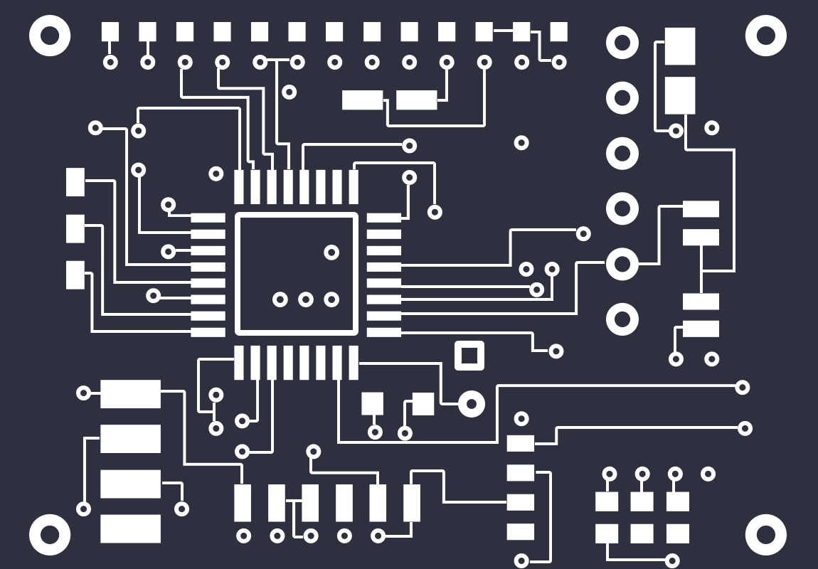
PCB
(
1
/
)
The preview image was not generated, please save it again in the
editor.
BOM
Project Members


 0
0
 0
0
Collect to album
Target complaint
Related Projects
Change a batch
Loading...
Add to album
×
Loading...
reminder
×
Do you need to add this project to the album?