


© 2024 EasyEDA Some rights reserved ISO/IEC
Editor Version
×
Standard

1.Easy to use and quick to get started
2.The process supports design scales of 300 devices or 1000 pads
3.Supports simple circuit simulation
4.For students, teachers, creators
Profession

1.Brand new interactions and interfaces
2.Smooth support for design sizes of over 5,000 devices or 10,000 pads
3.More rigorous design constraints, more standardized processes
4.For enterprises, more professional users
Ongoing
STD 24L01 modular
Mode: Editors' pick
- 3
Update time:
2021-04-08 20:45:40
Creation time:
2016-05-06 01:15:28
Description
1、Module description:
Emission data. First of all, the nRF24L01 configuration into firing patterns, then the address TX addr and TX data PLD according to the time from SPI write nRF24L01 buffer, TX PLD must in the CSN is low for writing, and TX addr in the launch write a can, and CE set for high level and maintain at least 10 microseconds, 130 microsecond delay after the emission data; if open automatic response, then nRF24L01 in sending data immediately enter the receive mode, receiving response signals. If you receive a response is considered the success of the communication, TX DS is set high, and TX PLD from sending the stack clear; if no response is received is automatically re emission the data (automatic retransmission has been opened), if the number of retransmissions (arc CNT) reaches the upper limit, Max RT set high, TX PLD is not clear; max RT or TX DS set high, the IRQ goes low to inform the MCU. Finally the successful launch, if CE is low, nRF24L01 enter standby mode 1; if send stack in data and CE is high, then enter the next launch; if there is no data to send in the stack and CE is high, enter standby mode 2.
When the data is received, the nRF24L01 is configured to receive mode first, and then 130 s is delayed to enter the receiving state to wait for the arrival of the data. When the receiver detects the valid address and CRC, the data packet is stored in the receiving stack, and the flag bit RX_DR is set at the same time, the IRQ becomes low, so as to inform the MCU to fetch the data. If the automatic response opens, the recipient is also entering the transponder signal state feedback. At the end of the final reception, if the CE becomes low, the nRF24L01 enters the idle mode 1.
2、Function Description:
•Worldwide 2.4GHz ISM band operation•250kbps, 1Mbps and 2Mbps on air data rates
•Ultra low power operation
•11.3mA TX at 0dBm output power•13.5mA RX at 2Mbps air data rate•900nA in power down •26µA in standby-I
•On chip voltage regulator•1.9 to 3.6V supply range•Enhanced ShockBurst™ •Automatic packet handling
•Auto packet transaction handling•6 data pipe MultiCeiver™
•Drop-in compatibility with nRF24L01
•On-air compatible in 250kbps and 1Mbps with nRF2401A, nRF2402, nRF24E1 and nRF24E2
•Low cost BOM
•±60ppm 16MHz crystal•5V tolerant inputs
•Compact 20-pin 4x4mm QFN package
3、Description of each function module:
![enter image description here][1]
4、Components and PCB diagram before welding:
![enter image description here][2]
5、Physical map after welding:
![enter image description here][3]
![enter image description here][4]
![enter image description here][5]
[1]: /editor/20160606/575514b2b6d82.png
[2]: /editor/20160606/575514d53628d.jpg
[3]: /editor/20160606/575514ef3fd3e.jpg
[4]: /editor/20160606/575514f74665c.jpg
[5]: /editor/20160606/5755153eee103.jpg
Design Drawing
schematic diagram
(
1
/
)
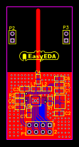
PCB
(
1
/
)
The preview image was not generated, please save it again in the
editor.
| ID | Name | Designator | Footprint | Quantity |
|---|---|---|---|---|
| 1 | 16M | X | 16m | 1 |
| 2 | 1M | R1 | 3-0603 | 1 |
| 3 | 22pf | C1,C2 | c-0603 | 2 |
| 4 | 1pf | C3,C4 | c-0603 | 2 |
| 5 | 3.3nH | L1 | 3-0603 | 1 |
| 6 | 10nH | L2 | 3-0603 | 1 |
| 7 | 2.2nf | C5 | c-0603 | 1 |
| 8 | 4.7pf | C6 | c-0603 | 1 |
| 9 | 22k | R2 | 3-0603 | 1 |
| 10 | 33nf | C7 | c-0603 | 1 |
| 11 | 10nf | C8 | c-0603 | 1 |
| 12 | 1nf | C9 | c-0603 | 1 |
| 13 | HDR2X4 | P1 | HDR2X4 | 1 |
| 14 | SIP2 | P2,P3 | HDR1X2 | 2 |
| 15 | NRF24L01+ | U1 | QFN20G-0.5-4X4MM | 1 |
Unfold
Project Members


 0
0
 3
3
Collect to album
Target complaint
Related Projects
Change a batch
Loading...
Add to album
×
Loading...
reminder
×
Do you need to add this project to the album?