


© 2024 EasyEDA Some rights reserved ISO/IEC
Editor Version
×
Standard

1.Easy to use and quick to get started
2.The process supports design scales of 300 devices or 1000 pads
3.Supports simple circuit simulation
4.For students, teachers, creators
Profession

1.Brand new interactions and interfaces
2.Smooth support for design sizes of over 5,000 devices or 10,000 pads
3.More rigorous design constraints, more standardized processes
4.For enterprises, more professional users
Ongoing
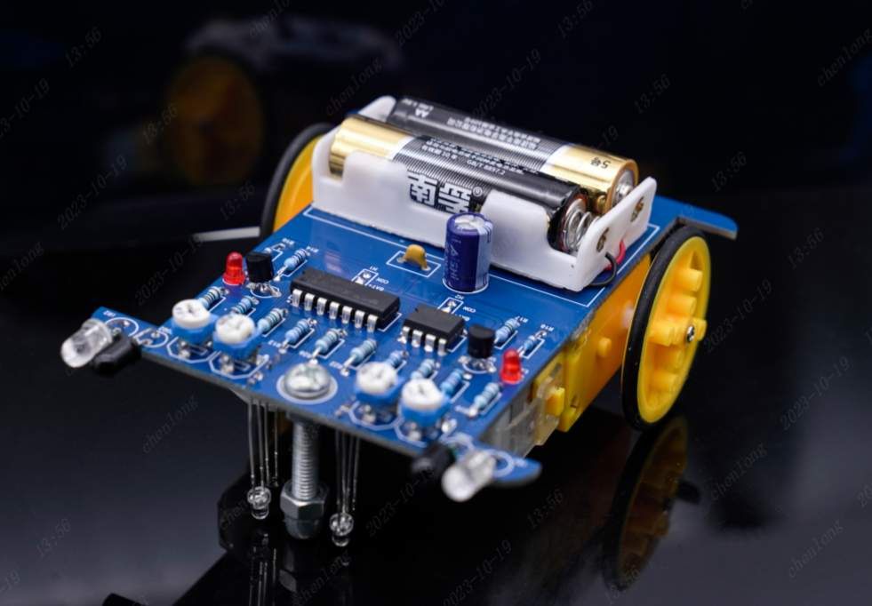
PRO Digital-Analog Tracking and Obstacle Avoidance car
License: Public Domain
Mode: Editors' pick
- 2
Update time:
2024-01-30 03:21:49
Creation time:
2023-11-03 07:50:49
Description
1 Design requirements
Design a simple line tracking obstacle avoidance car, requires the use of digital circuits to achieve tracking function, analog circuits to achieve obstacle avoidance function.
2 Overall design program
According to the design requirements, the use of 74HC00N NAND gate with infrared tube, determines conduction or not by whether the receiver tube detects infrared light or not. Signal input NAND gate achieving digital circuit tracing
Using LM393 Comparator with Infrared tube also aim at determines conduction or not by whether the receiver tube detects infrared light or not. Input two sets of signals into the comparator to achieve the analog circuit obstacle avoidance function
3 circuit composition
3.1 Power supply circuit
The use of two 5 dry cell batteries for power supply, each dry cell 1.5V, two in series is 3V, to meet the minimum power supply needs of the chip, through the three-position slide switch to achieve trajectory, obstacle avoidance function of switching. C1, C3 capacitor for the filter storage capacitor, when the motor starts to work, transient currents are large, and the 100uF capacitor can assist the battery to discharge.

3.2 Motor Driving Circuit
The positive pole of the battery is connected to the positive pole of the motor, and the negative pole is controlled to conduct through the transistor, so that when the digital tracking or analog obstacle avoidance signal is generated, the base pole of the transistor is controlled so as to realize the control of the left and right tires, and realize the tracking and obstacle avoidance functions.

3.3 Digital Signal Tracking
U2 and U3 are infrared transmitter tubes, and LED3 and LED4 bit corresponding infrared receiver tubes, which are installed on both sides of the front wheels of the car. The principle is analyzed as follows:
1, when the car starts to move when it touches the white paper, infrared light reflection, is received by the receiver tube, the receiver tube conduction, touches the black line when the infrared light is absorbed, the receiver tube cutoff;
2, 74HC00N is with the non-gate, when you touch the black line, the receiver tube cutoff, CNT1 output high level, corresponding to OUT1 output low level, OUT3 output high level;
3, at this time, OUT3 output high level will flow through the motor transistor, control the three-stage conduction, motor rotation;
Vehicles in the map route constantly touch the black line and white line, thus constantly on and off transistor, to realize the black line around the track patrol function

3.4 Analog Signal Obstacle Avoidance
IR1 and IR2 are infrared transmitter tubes and CGQ1 and CGQ2 are the corresponding infrared receiver tubes, which are installed on both sides of the front of the vehicle. The schematic diagram is analyzed as follows:
1, when the car is running, there is no obstacle in front of the car, the infrared transmitter signal will not be received, the receiver tube is cut off, the 393 comparator isotropic input is the battery voltage, the voltage is greater than the inverted input, at this time, the 393 comparator outputs a high level, controlling the vehicle to run forward.
2、When there is an obstacle in front of the vehicle, the infrared emitting signal is received by the receiver tube, the receiver tube conducts, the 393 comparator is low at the same input, the voltage is less than the inverted input, at this time, the 393 comparator outputs a low level, and the corresponding wheel stops running, so as to realize the steering.

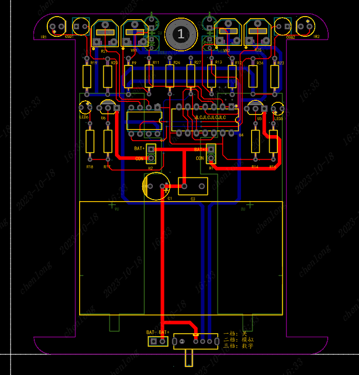
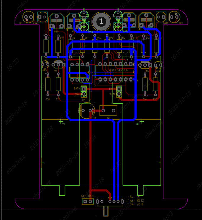
4 PCB design
After completing the schematic design, first pay attention to check whether the circuit is connected to the right, whether there is a missing network is not connected to the situation. After all the checks are correct, click Design - Schematic to PCB in the menu bar at the top of the schematic to start PCB design.
4.1 Outline Design
After generating the PCB, you need to set a PCB shape, the size of the shape needs to be based on the number of components and the size of the shell design, adhering to the size of the right, beautiful principle, the project in the design of the shape, you need to take into account the position of the motor and the tires, to ensure that the tires and the PCB board will not interfere.
4.2 Component Layout
Schematic devices transferred to the PCB after the component layout is relatively chaotic, the second step in the design of PCB components need to be categorized and layout, classification is based on the placement of the devices of each circuit, the use of Jialitron EDA provides a layout transfer function can be very quickly on each circuit module layout, pay attention to the infrared alignment tube should be placed on the edge of the board, to reduce unnecessary interference.

4.3 PCB Wiring
PCB alignment is divided into top-layer alignment and bottom-layer alignment when designing a double-layer circuit board, in which the bottom-layer alignment is red by default and the bottom layer is blue, and the alignment is also connecting copper wires in the circuit board. Just select the layer in Layer and Element and then connect the pads of two identical networks. Seemingly simple connection, but also need to constantly adjust and optimize, the placement of components layout will also affect the difficulty of the alignment, in the layout of a little more consideration of the alignment will be much simpler, in the alignment to provide the following points of reference recommendations:
(1) The power line is set to 40mil, the signal line is set to 10mil;
(2) alignment priority to consider the top layer alignment, the top layer can not be smoothly connected to consider the bottom layer alignment;
(3) GND does not need to be routed directly to the bottom layer of copper can be;
(4) The alignment process gives priority to straight lines, the need to bend places to blunt corners or arc bends;
(5) After the completion of the alignment to add the appropriate silkscreen marking to explain the purpose of the PCB board and interface functions
5 Debugging Note
1、After the welding is completed, do not insert the battery first, first use the multimeter to test whether it is short-circuited by using the on-off gear;
2、When it is found that the vehicle operation can not realize the purpose, by adjusting the value of the adjustable resistor, so as to change the sensitivity;
3、You can test each input voltage value by multimeter, so as to know the corresponding voltage change more clearly;
4, in the purchase of the chip, you need to pay attention to the 3V battery to meet the minimum operating voltage of the chip, if not, you can try to use three batteries for series connection
Design Drawing
schematic diagram
(
1
/
)
PCB
(
1
/
)
The preview image was not generated, please save it again in the
editor.
BOM
Project Members


 1
1
 2
2
Collect to album
Target complaint
Related Projects
Change a batch
Loading...
Add to album
×
Loading...
reminder
×
Do you need to add this project to the album?