


© 2024 EasyEDA Some rights reserved ISO/IEC
Editor Version
×
Standard

1.Easy to use and quick to get started
2.The process supports design scales of 300 devices or 1000 pads
3.Supports simple circuit simulation
4.For students, teachers, creators
Profession

1.Brand new interactions and interfaces
2.Smooth support for design sizes of over 5,000 devices or 10,000 pads
3.More rigorous design constraints, more standardized processes
4.For enterprises, more professional users
Ongoing
STD Analog to digital converter
Mode: Editors' pick
- 0
Update time:
2021-04-10 10:46:50
Creation time:
2015-09-14 07:47:59
Description
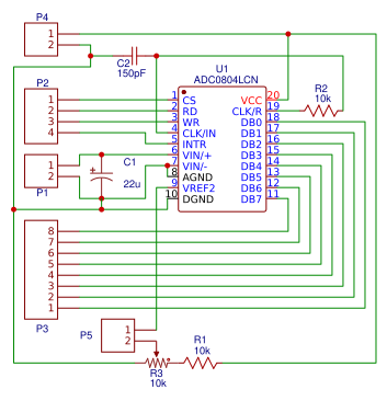
**Analog to digital converter.**
This project is about a simple analog to digital converter based on the ADC0804 IC. ADC0804 is an 8-bit ADC with adjustable step size. It is very easy ti interface it to microcontrollers. In face am ADC circuit like this one is very essential for designing systems based on microcontrollers like 8051 which does not have a built in ADC.
**About the circuit.**
Resistor R2 and capacitor C2 are associated with the clock circuit of the ADC. Preset resistor R3 is used for adjusting the Vref/2 voltage of the ADC. The step size of the ADC depends on the voltage we give at the Vref/2 pin of the ADC. The table given below shows different Vref/2 values and corresponding step sizes.
![enter image description here][1]
Input voltage is applied across Vin+ and Vin- pins of the ADC. Capacitor C1 is used to by-pass any noise or fluctuation present in the input voltage. If this capacitor is not used, the ADC output will not be stable for fastly varying inputs. Digital output is available across D0 to D7 pins of the ADC.
Control signals are given to CS, RD, RW and INTR pins of the ADC. To make a conversion by the ADC, CS is made 0 and a low to high transition is given to WR pin. The INT pin will become zero if the conversion is finished. The CS is made 0 and a high to low transition is given to WR pin for reading the data from the ADC. Photo graph of the ADC board connected with an 8051 based voltmeter circuit is shown below.
![enter image description here][2]
[1]: /editor/20150910/55f18b8050f10.png
[2]: /editor/20150914/55f6a068baf15.png
**Program.**
The code for the voltmeter is given below.
ORG 00H
RS EQU P2.7
RW EQU P2.6
E EQU P2.5
MOV DPTR,#LUT
MOV P1,#11111111B
MOV P0,#00000000B
MOV P3,#00000000B
MOV P2,#00000000B
MAIN: CLR P3.7
SETB P3.6
CLR P3.5
SETB P3.5
WAIT: JB P3.4,WAIT
CLR P3.7
CLR P3.6
MOV A,P1
MOV B,#10D
DIV AB
MOV R3,B
MOV B,#10D
DIV AB
MOV R2,B
MOV R1,A
ACALL DINT
ACALL VOLT
ACALL TEXT
SJMP MAIN
VOLT: MOV A,R3
ACALL ASCII
ACALL DISPLAY
MOV A,R2
ACALL ASCII
ACALL DISPLAY
MOV A,R1
ACALL ASCII
ACALL DISPLAY
RET
TEXT:MOV A,#" "
ACALL DISPLAY
MOV A,#"V"
ACALL DISPLAY
MOV A,#"o"
ACALL DISPLAY
MOV A,#"l"
ACALL DISPLAY
MOV A,#"t"
ACALL DISPLAY
MOV A,#"s"
ACALL DISPLAY
RET
DINT:MOV A,#0FH
ACALL CMD
MOV A,#01H
ACALL CMD
MOV A,#06H
ACALL CMD
MOV A,#83H
ACALL CMD
MOV A,#3CH
ACALL CMD
RET
CMD: MOV P0,A
CLR RS
CLR RW
SETB E
CLR E
ACALL DELAY
RET
DISPLAY:MOV P0,A
SETB RS
CLR RW
SETB E
CLR E
ACALL DELAY
RET
DELAY: CLR E
CLR RS
SETB RW
MOV P0,#0FFh
SETB E
MOV A,P0
JB ACC.7,DELAY
CLR E
CLR RW
RET
ASCII: MOVC A,@A+DPTR
RET
LUT: DB 48D
DB 49D
DB 50D
DB 51D
DB 52D
DB 53D
DB 54D
DB 55D
DB 56D
DB 57D
END
Design Drawing
schematic diagram
(
1
/
)
PCB
(
1
/
)
The preview image was not generated, please save it again in the
editor.
| ID | Name | Designator | Footprint | Quantity |
|---|---|---|---|---|
| 1 | ADC0804LCN | U1 | DIP20 | 1 |
| 2 | 22u | C1 | CP_8X13MM | 1 |
| 3 | SIP4 | P2 | HDR1X4 | 1 |
| 4 | SIP2 | P1,P4,P5 | HDR1X2 | 3 |
| 5 | SIP8 | P3 | HDR1X8 | 1 |
| 6 | 10k | R2,R1 | R3 | 2 |
| 7 | 150pF | C2 | C1 | 1 |
| 8 | 10k | R3 | TRIM_POT_PTH | 1 |
Unfold
Project Members


 0
0
 0
0
Collect to album
Target complaint
Related Projects
Change a batch
Loading...
Add to album
×
Loading...
reminder
×
Do you need to add this project to the album?