

 Ongoing
High side bidirectional blocking PMOSFET switch
STDHigh side bidirectional blocking PMOSFET switch
License
:Public Domain
Description
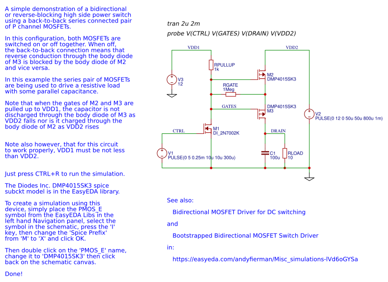
A simple demonstration of a bidirectional
or reverse-blocking high side power switch
using a back-to-back series connected pair
of P channel MOSFETs.
In this configuration, both MOSFETs are
switched on or off together. When off,
the back-to-back connection means that
reverse conduction through the body diode
of M3 is blocked by the body diode of M2
and vice versa.
In this example the series pair of MOSFETs
are being used to drive a resistive load
with some parallel capacitance.
Note that when the gates of M2 and M3 are
pulled up to VDD1, the capacitor is not
discharged through the body diode of M3 as
VDD2 falls nor is it charged through the
body diode of M2 as VDD2 rises
Note also however, that for this circuit
to work properly, VDD1 must be not less
than VDD2.
Just press CTRL+R to run the simulation.
The Diodes Inc. DMP4015SK3 spice
subckt model is in the EasyEDA library.
To create a simulation using this
device, simply place the PMOS_E
symbol from the EasyEDA Libs in the
left hand Navigation panel, select the
symbol in the schematic, press the 'I'
key, then change the 'Spice Prefix'
from 'M' to 'X' and click OK.
Then double click on the 'PMOS_E' name,
change it to 'DMP4015SK3' then click
back on the schematic canvas.
Done!
See also:
Bidirectional MOSFET Driver for DC switching
and
Bootstrapped Bidirectional MOSFET Switch Driver
in:

BOM
| ID | Name | Designator | Footprint | Quantity |
|---|---|---|---|---|
| 1 | PULSE(0 5 0.25m 10u 10u 300u) | V1 | 2P-5.0 | 1 |
| 2 | PULSE(0 12 0 50u 50u 800u 1m) | V2 | 2P-5.0 | 1 |
| 3 | 10 | RLOAD | R3 | 1 |
| 4 | DMP4015SK3 | M3,M2 | NONE | 2 |
| 5 | DI_2N7002K | M1 | 1 |
 Clone
CloneProject Members
 Empty
Empty
Comment