

 Ongoing
PCB Board Design
STDPCB Board Design
License
:Description
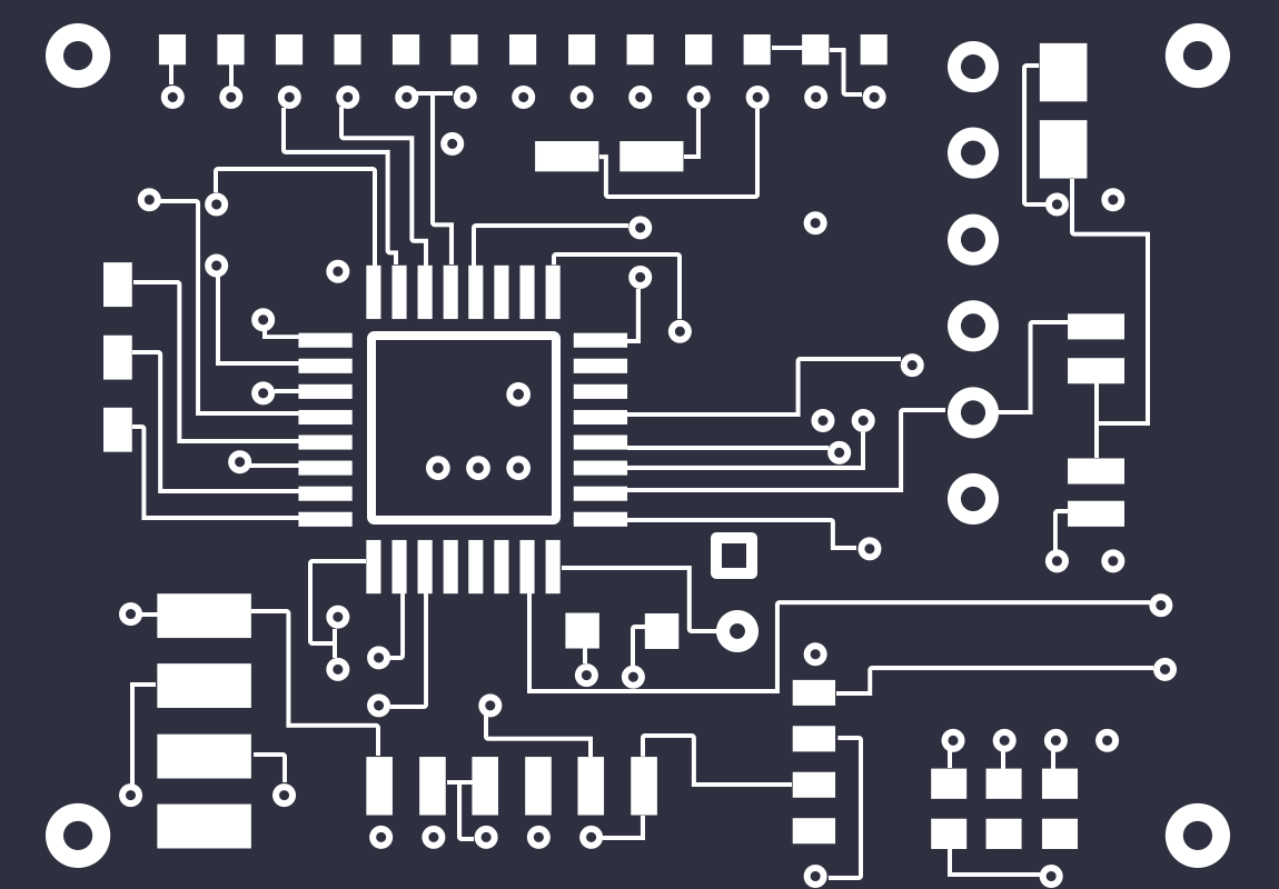
How to create your own Arduino (UNO) shield PCB board very easily using EasyEDA. I will be creating a Arduino UNO 3 x 3 x 3 LED Cube Shield with the built-in spice tool which you could create schematics, design PCB boards, generate a bill of materials and even analyze your circuits.
Preparation
The easiest way to start practicing is by using someone else’s schematic since this will save you time, which means you have more time to work on your PCB board design skills. Feel free to fork the LED Cube Shield project if you’re interested and want to completely follow the following steps.
The model for the Arduino Shield PCB board can be found in the online library.

Step 1 - converting your schematic to PCB:
Open up your schematic and click on “Convert project to PCB” :

Step 2 - Placing the components:
You will end up with a screen filled with an outline (the purple line) and with all the components you placed down in your schematics.
Start dragging the components to where you want them to be. Make sure to place the components on the inside of the Arduino shield.
Step 3 – Drawing a custom outline:
Now we can draw the outline. I always like to use the same size shield as the Arduino itself, so I draw my new outline precisely on the outline of the Arduino shield PCB board.
To draw the outline you have to switch to the “BoardOutline” layer in the layers menu:

Click on the current outline (the pink square in your editor) and press delete to get rid of it.
Use the tools shown above to draw your new outline.
Once you’re done with your outline you can switch back to either the top or bottom layer.
Step 4 - Routing:
Since the Arduino has a lot of data pins we don’t need a GND copper area.
The Arduino isn’t capable of providing a lot of current, so this means we won’t have to draw very thick tracks.
You could choose to either: Auto Route or route everything yourself.
The Auto Router function can be found here:


We are going to route everything ourselves. This can be done by clicking on the track tool in the tools menu. Once you click on the pad of one component and move your pointer around you should see a track appear on the PCB board and the small blue lines should move with your pointer.
To connect 2 components together you have to follow the blue line and route your track around holes and other components until it reaches the other component. If you did this successfully the blue line should disappear.
Do this for all your components until you see no more blue lines. If you use SMD components and have to switch to another layer make sure to use VIA’s which can be found in the tools menu since a SMD component only has pads on one layer.
Step 5: Adding holes
To secure the shield onto your Arduino we have to add holes. Now in my case I didn’t have to do this, since the Arduino model already had holes included.
This is how you can add holes if your model doesn’t include holes:
Click on the “Hole” tool in the tools menu. Set the size in the toolbar on the right.
Make sure you’re using the right units!!
Once the size has been set you can click on the PCB board to place your holes down.
Step 6: Adding Text labels to the PCB board
To add text click on the “Text” tool in the tools menu. Place the text where you want it to be and change the text in the right properties menu. This could be extremely useful if you have to connect external modules to your shield since all the pins are marked however you want yourself.

You can also change to the desired silk layer in the toolbar on the right. After you finished your PCB design, you can directly order PCBs from the same tool and calculate your PCB price quickly with the online pricing calculator.
Step 7: Prototype PCB

The order steps process is also simple, here are the PCB order steps:
Just click the Fabrication Output button in the PCB editor or Upload your gerber files on PCB order page;
Fill in your PCB information;
Add to cart;
Get your PCBs.
Design Drawing
BOM
 Clone
CloneProject Members
 Empty
Empty
Comment