

 Ongoing
Getting Started with EasyEDA Part 3: PCB Layout
STDGetting Started with EasyEDA Part 3: PCB Layout
License
:Description
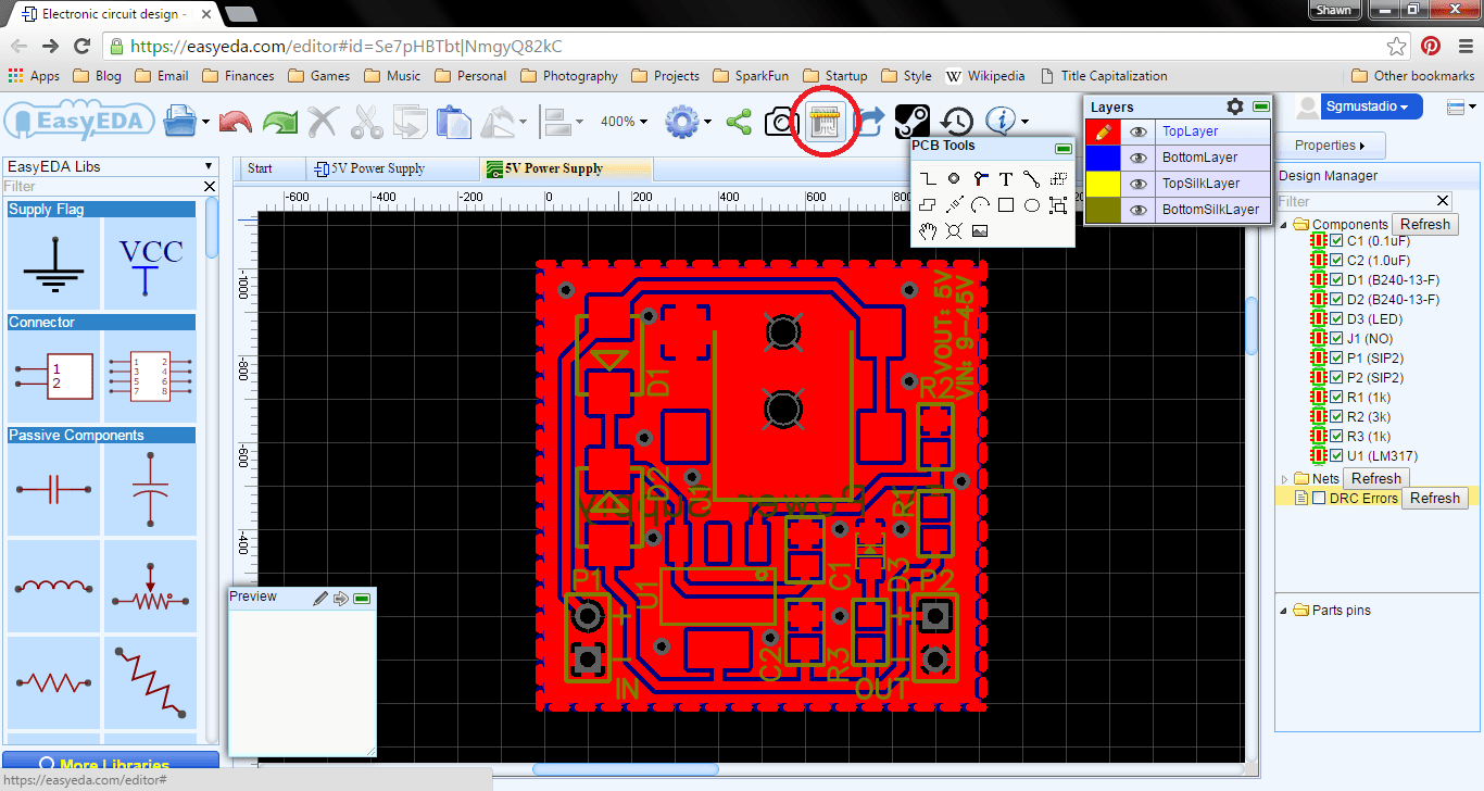
Exporting Schematic to PCB
Last week, we finished creating our schematic. In your schematic, click on the Convert Project to PCB… button.

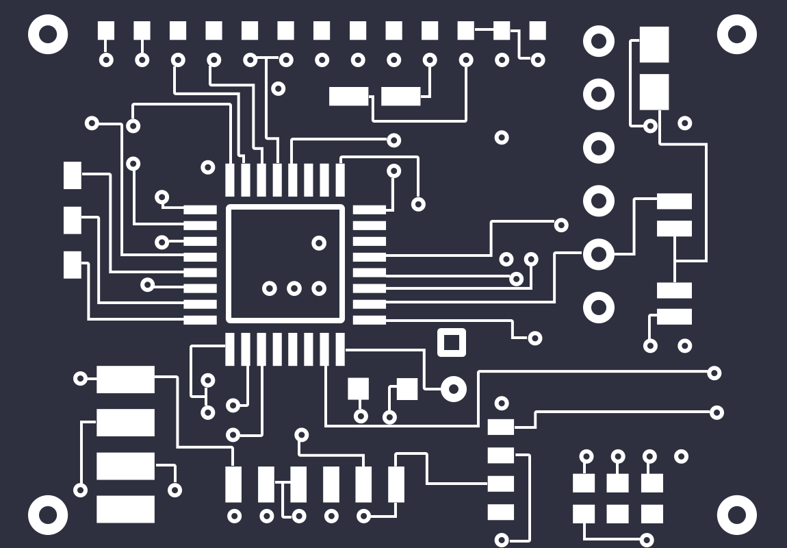
You should be presented with an initial board outline and your components connected by air wires.

Note that we will layout the PCB in mils, even though we created package footprints in mm.
Component Placement
Go ahead and delete the purple board outline.

Drag the components into a nicely packed area. Try and avoid having air wires cross as much as possible (press r to rotate the part). If it helps, I’ve listed the X, Y, and rotation parameters for each component. You don’t need to use my placement, but I found that this arrangement allows for all traces to be placed on the top layer.
Part X Y Rotation
C1 600 -390 270
C2 600 -200 270
D1 150 -800 90
D2 150 -450 270
D3 750 -350 90
J1 550 -1050 270
P1 100 -100 90
P2 900 -200 270
R1 900 -450 90
R2 900 -650 270
R3 750 -200 270
U1 400 -250 180

Draw Board Outline
Select Track from the PCB Tools box and BoardOutline from Layers.

Draw a square of 1000 mils by 1000 mils around the components, clicking on each corner to start a new line. Once you click on the final corner, right-click to stop placing track.

Set Design Rules
Before placing traces, we want to set our design rules. These can often be found from the PCB fab house’s website. For our purposes, we want to make the spacing a bit bigger than the defaults. Select the drop-down list on the far right of the page. From that, select Miscellaneous and Design Rule Settings…

Change all the values to 10 (mils), except for “Via Hole Size,” which we’ll change to 20. Realtime DRC offers the ability to show errors on the layout as they occur. This is a very handy feature, so I recommend leaving it enabled.

Click Setting, and close the Design Rule Setting window.
Drawing Traces
Click on Track in the PCB Tools box, click in the red box of TopLayer to draw in the top layer, and change the Routing Width in the Other category on the right side to 20. Click on pin 2 of P1 to start drawing a trace. You should see a white dot appear when you have a trace connected to the pin.

You should see the air wire (blue line) move as you draw the trace. It will show you where to connect the trace. When you have reached a correct pin, a white dot will appear. Click to end the trace.

We want to connect the other pads with traces, but we want to leave GND unconnected (we will connect GND with a ground pour later). To turn off the GND air wires, click the Design Managerstrong text button in the right-side pane, drop down the Nets category, and deselect GND.

Go ahead and use the Track tool to connect the rest of the pads, as shown by the blue air wires. You should be able to do it on one layer. If you need to switch to another layer, just click on the layer (e.g. BottomLayer) from the Layers box. This will automatically drop a via and let you keep routing on that layer.

Ground Pour
In PCB Tools, click the Copper Area button. Make sure that TopLayer is selected. Draw a box around the board outline (it can be on top of or just outside the purple square).

Right-click to end the outline. The pour will automatically fill in. Press esc to exit the tool, and click on the pour’s outline to select it. Change Net to GND, and make sure Clearance is set to 10mil. Click Rebuild CopperArea.

Repeat this whole process for the BottomLayer. You can click on the eye icons by the layers to turn the visibility of the top off and on.

Ground Vias
To reduce inadvertent RF transmissions and reception, we connect our top and bottom pours with vias. Granted, this is a DC board, but it is generally considered good practice to stitch the pours together.
Click the Via tool in PCB Tools. View and edit the TopLayer. Click to place the via in the top-left corner of the board, ensuring that it does not touch a component’s pad or a trace. Press esc to stop placing vias. Select the via you just placed and change its attributes:
Diameter: 40mil
Hole(D): 20mil
Net: GND

Repeat this process to place a few more vias around the board, connecting the ground pours.

Silk Screen Labels
Click on the individual component reference designators (RefDes), such as R1, and move them so that they do not overlap any components or vias. Adjust their rotation to 0 or 90 so that they all face one of two directions.

Using the Text tool and TopSilkLayer, denote IN vs. OUT. Also, add + and – markers to the appropriate pins. Change the text attributes so that the Height is 45mil.

Add some text to show what the input and output voltages are. Note that we changed the Height parameter to 35mil.

Add the name of our board (e.g. “5V Power Supply”) to the BottomSilkLayer. Note that we changed the Height to 70milstrong text.

Design Rules Check
We’re done! Well, almost. Before we send out the board for fabrication, we should run a Design Rules Check (DRC) to make sure we’ve connected everything, there are no touching traces, etc.
In the right-side pane, click the Design Manager button. Next to DRC Errors, click Refresh. If there are any errors, you will see them appear.

For example, if we move the top trace down so it touches the barrel jack footprint and refresh DRC, we will see actual errors appear.

Make sure you fix all your DRC errors. Click on each error to highlight the problem area. Once you have everything fixed, select File > Save As. Give it an appropriate name and description.

Send Your Board out for Production
In the toolbar, click on the Fabrication Output… button.
This will open up a new browser window. Ensure the board parameters are to your liking. The defaults are good for prototyping–just note that the basic HASL finish has lead in it, so choose “HASL (lead-free)” if you don’t want that.

If you want to use a different fab house, you can click Download Gerber Files. This will download a .zip file containing the files needed by most production facilities. You can verify the files with a free viewer like gerbv.
If you decide to buy through EasyEDA, click Save to Cart, and follow the rest of the instructions to fill out the shipping and billing data.

Once you have placed your order, wait a few weeks, and your boards should arrive at your doorstep!
Conclusion
You’ve just created a complete board with EasyEDA! Certainly, these tutorials did not cover all the features within EasyEDA, but at least you have an idea of what’s needed to create a PCB from start to finish. For example, one tool we did not cover was EasyEDA’s built-in SPICE program. This lets you simulate circuits without needing to build them.
A video about PCB design will helpful to you by https://easyeda.com/Doc/Tutorial/PCB.htm#PCB-Design-Editor
To view EasyEDA’s official documentation and tutorials, see https://easyeda.com/Doc/Tutorial/
Design Drawing
BOM
 Clone
CloneProject Members
 Empty
Empty
Comment