Platform for creating and sharing projects - OSHWLab
Activity
More
We invite all electronics enthusiasts to participate in the eventand share your open-source hardware designs. We can cover all the manufacturing fees with the following services: Free PCB/SMT/3D/CNC/MC/Multi-color silkscreen.
OSHWLab Stars
2023-01-01 ~ 2026-12-31in progress

If you are a non-profit organization using EasyEDA Pro for your PCB designs, we invite you to reach out and explore collaboration opportunities with us.
Collaborate with EasyEDA
2024-12-28 ~ 2026-12-28in progress

Receive $20 to $2000 worth of materials to aid your projects. 1. Create video tutorials about EasyEDA Pro (project design sharing, user experience, etc.) 2. Publish on YouTube
Video Creator Program
2024-08-31 ~ 2026-12-31in progress
Collections
More

188 project in total
Enter the Collection >
32 project in total
Enter the Collection >

Videos
MoreForums
MoreActivity
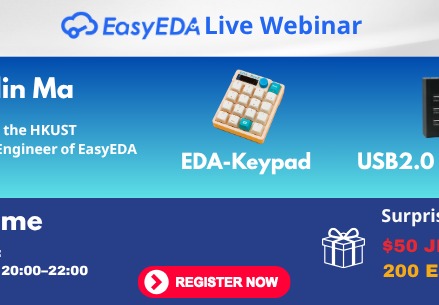
EasyEDA Live Webinar – Learn PCB Design & Win Prizes!
Latest Reply:
7 days agogreat thank you i will sure join and learn about it
Project
How to download a project from OSHWHUB?
Latest Reply:
6 days agoOthers
Photoresistor circuit.
Latest Reply:
6 days agoHello, I am not sure but I don't think that my post is in the good forum. I wanted to know if my circuit seems to be correct or no. Have a good day.
Schematic
How to Add a Decoupling Capacitor Between IC Power Pins Without Joining Global Nets in EasyEDA Pro
Latest Reply:
a day agoYou may find this topic from the old forum helpful:
https://easyeda.com/forum/topic/Understanding-Ratlines-371bdbf646c54b23a57451eb05b2026d
In EasyEDA, any net that is connected to any other net purely by copper can only have one netname. There is no way to distinguish between two parts of the same net by naming them separately.
So a net in the schematic is the same net everywhere it appears even if the connection is not made by wire but by netlabel. Similarly, a net in the PCB is the same net everywhere it appears even if the connection is made by different width tracks or any combination of tracks, copper areas and vias.
Nets can only have different names if they are physically separated even if only by a zero ohm resistor or a wire link. So, for example a so-called Analogue VDD and a Digital VDD connection to a chip can only have separately named nets going to them if there is a physical component in series somewhere that separates them. f the two pins are joined purely by copper, no matter how, then they must be connected together by the same net name. The same is true of course for ground connections.
Note that the net link symbol in EasyEDA Pro does not appear to actaully function as a net splitter.
Featured Articles
More Activity
Materials application instructions
Introduction: Only support "OSHWLab Stars" projects.
The order amount cannot exceed $5,000
 Technique
Roll the Future: Create Smart Timer Dice
Introduction: Welcome to OSHWLab Weekly: Create, Innovate, Explore. Discover projects and master EasyEDA!
 Technique
Ordering Boards for OSHWLab Projects
Introduction: Are you new to this hobby, do you want to replicate a community project? Here's the easy way


