You need to use EasyEDA editor to create some projects before publishing
Guide to Panelization of Board for PCB Assembly
15472 38
Banjobeni 3 years ago
This guide is relevant if you want the following: * panelize a PCB design, and * have a ground plane (copper fill) * use SMT assembly at JLCPCB It covers a shortcoming (unsuitable for ground plane (copper fill)) of [https://docs.easyeda.com/en/PCB/Panelize/index.html#Panelize-by-Manually](https://docs.easyeda.com/en/PCB/Panelize/index.html#Panelize-by-Manually) I wrote this guide so I don't have to reinvent the wheel next time I need one. I have sucessfully used it and confirmed that the PCBs ordered with assembly work as I intended. However, I will not take any responsibility for the correctness of this guide. USE AT YOUR OWN RISK. Based on at least one EasyEDA hack/bug, so it may cease to work with newer versions. Tested on V6.3.43. 
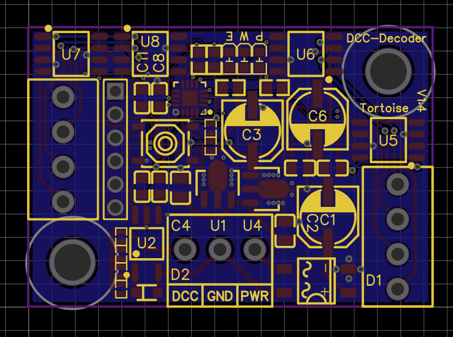
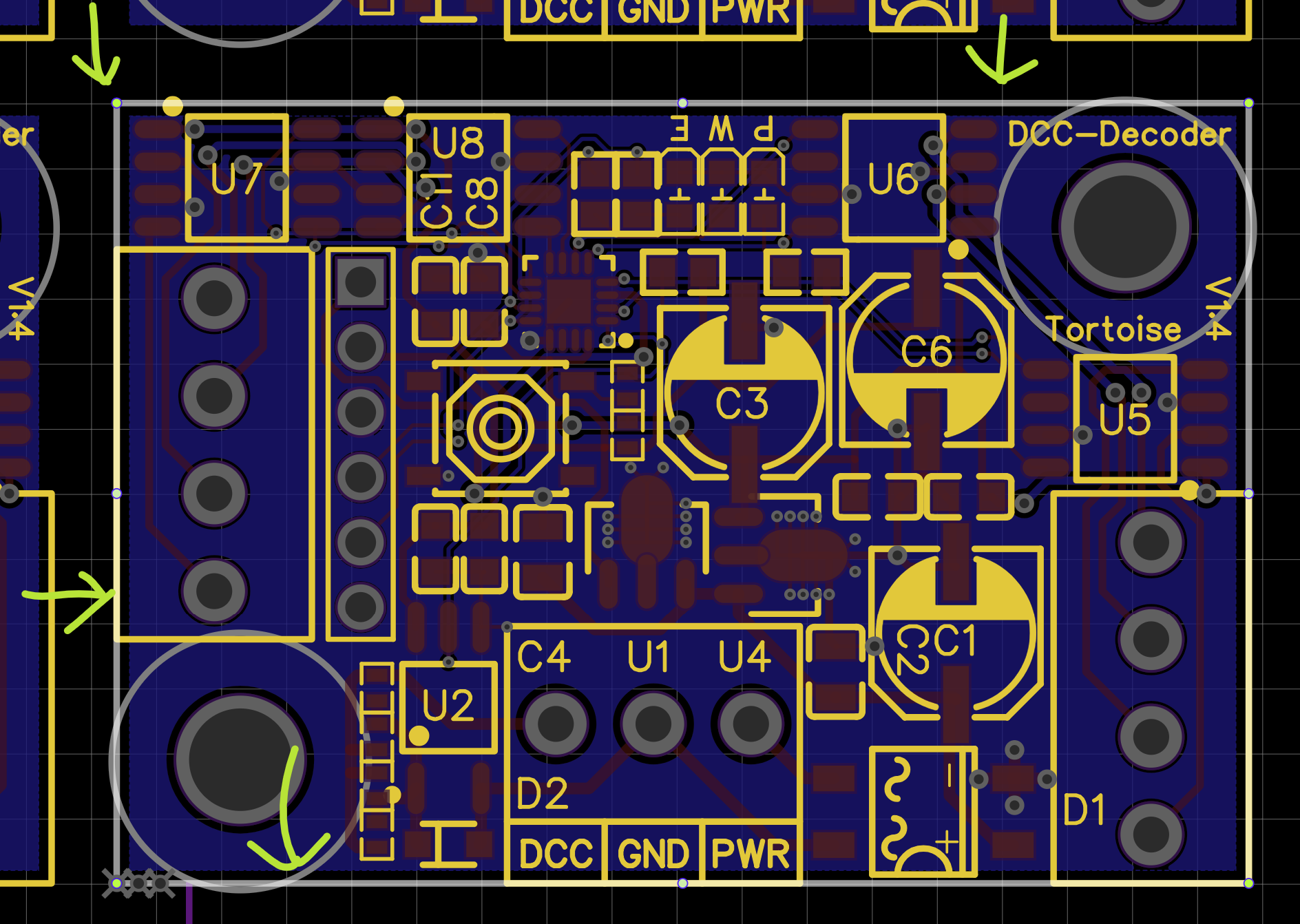
1\. Fully design and finish your single board\, including DRC\. ![image.png](//image.easyeda.com/pullimage/CXvPbSPXpRo30ANGvKov7VsmgqJyAfI9bNSFUW37.png) 
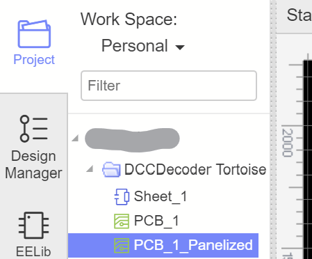
2\. Clone PCB design to new file \(named XY\_Panelized\) in same project\. ![image.png](//image.easyeda.com/pullimage/pDe3TRRr5WSt99wspwTielvWjIHTqFXXEo3n9Ck1.png) 3\. Use the built\-in "Panelize" function to initially panelize the board\. ![image.png](//image.easyeda.com/pullimage/dfiZQgrdfVO8U1JWr9dTS3HiXzk4xNq24iEJTiSA.png) ![image.png](//image.easyeda.com/pullimage/RvVg1kzU2sXgv0vLwkupV0Q5AJwciaqPsFRbwQ9T.png) 
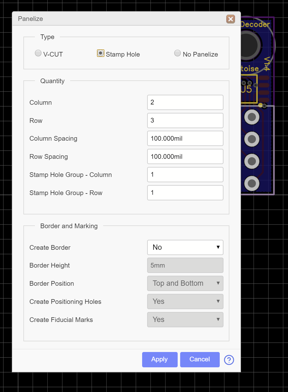
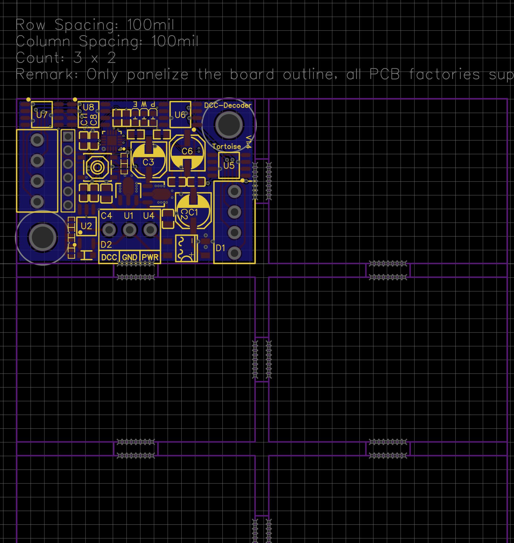
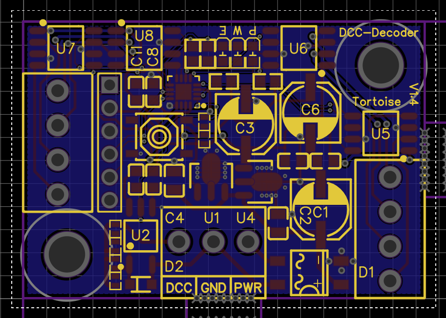
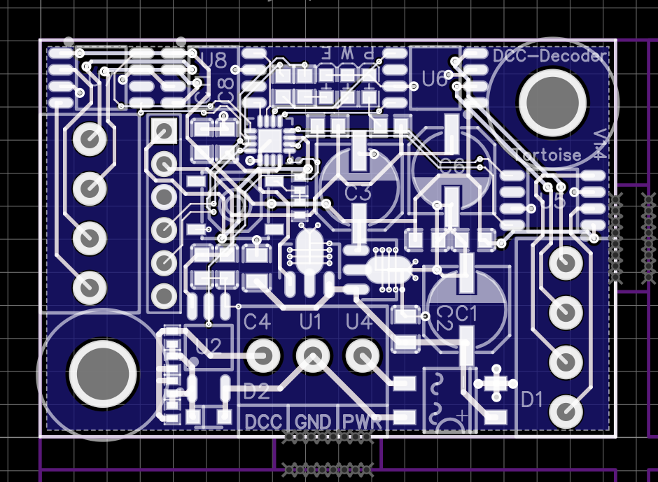
Note that only the outline is panelized. All the components and layout are not copied. Let's call the upper left board that has all the components and layout the "primary board". 
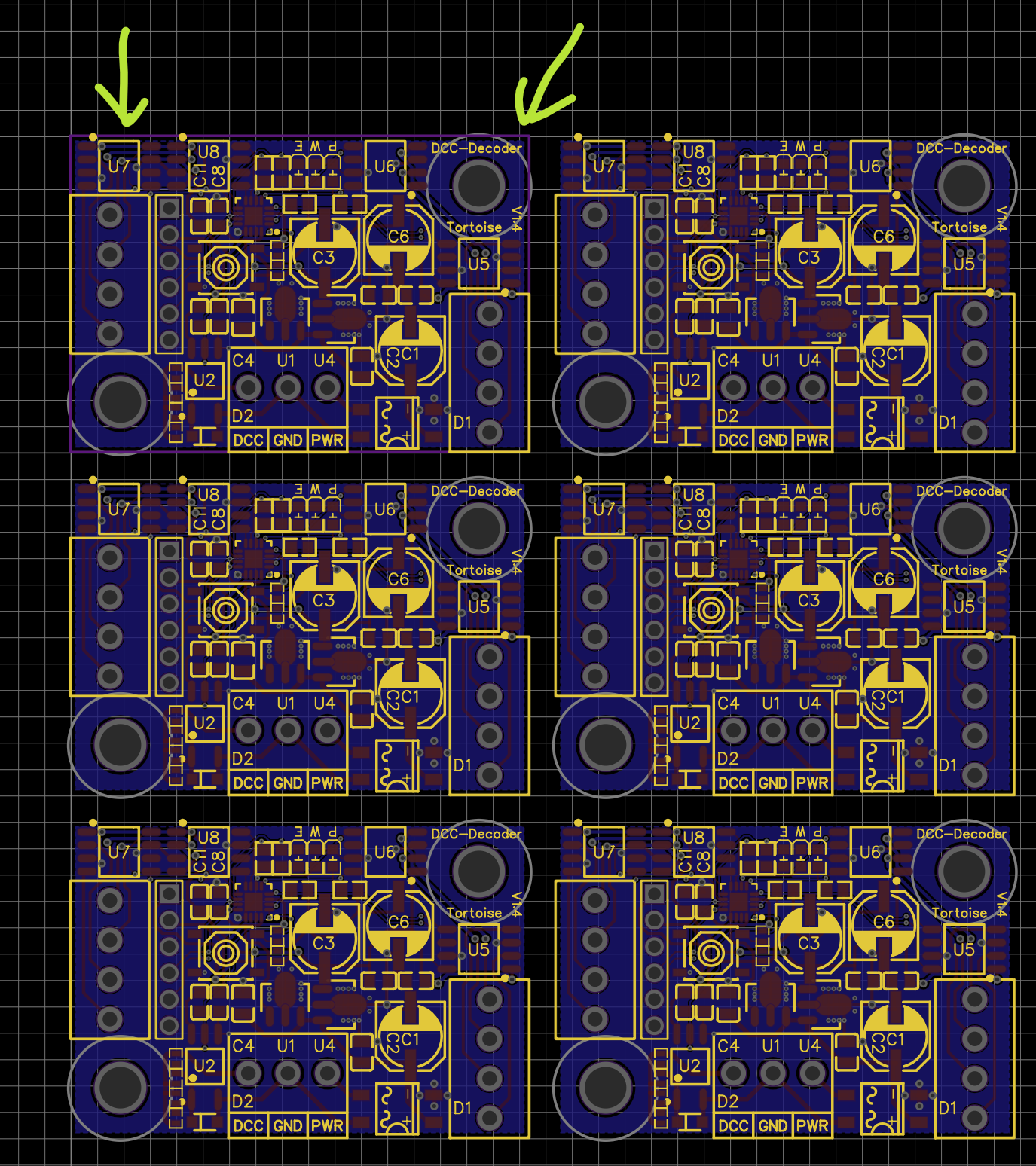
4\. Clone the primary board to all secondary boards\. Select the complete primary board including outline\. ![image.png](//image.easyeda.com/pullimage/FrvzsuZg4QN34xntbqc9Glh8Y0USGoCtefjpUPXb.png) ![image.png](//image.easyeda.com/pullimage/Ozorw9ZYCQORQeHiukThyexawD62MTwNmjO08d1c.png) 6\. Use Ctrl\+Shitf\+C to copy by reference point\. Use the upper left corner as reference point\. Make sure you hit the corner of the primary board outline exactly\, zoom in as needed\. ![image.png](//image.easyeda.com/pullimage/iVcWJcRtdn0PY3LvxQJtWsNNsNBJWyZM9SPKFeU5.png) 
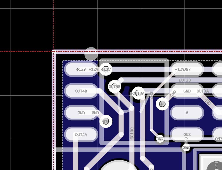
7\. Use Ctrl\+Shift\+V to paste by reference point\. Again\, make sure that you hit the corner of the secondary board exactly\. ![image.png](//image.easyeda.com/pullimage/co9dlNHW2Vv9cxvtQ3NNfKi4yph0qOTTLh6tYzsn.png) 8\. If everything is done correctly\, all of the primary board including the copper area is copied\. Note that since we enabled panelization \*and\* we also copied the outline of the primary board\, the panelization will be extended and look wrong\. We will fix this later\. \(Copying outline in this step is \*required\* because otherwise the copper area will not copy correctly\!\) ![image.png](//image.easyeda.com/pullimage/pfiOJgk2av5LhJzknwWbcxJMRAaxaZT2dy28FRCJ.png) 
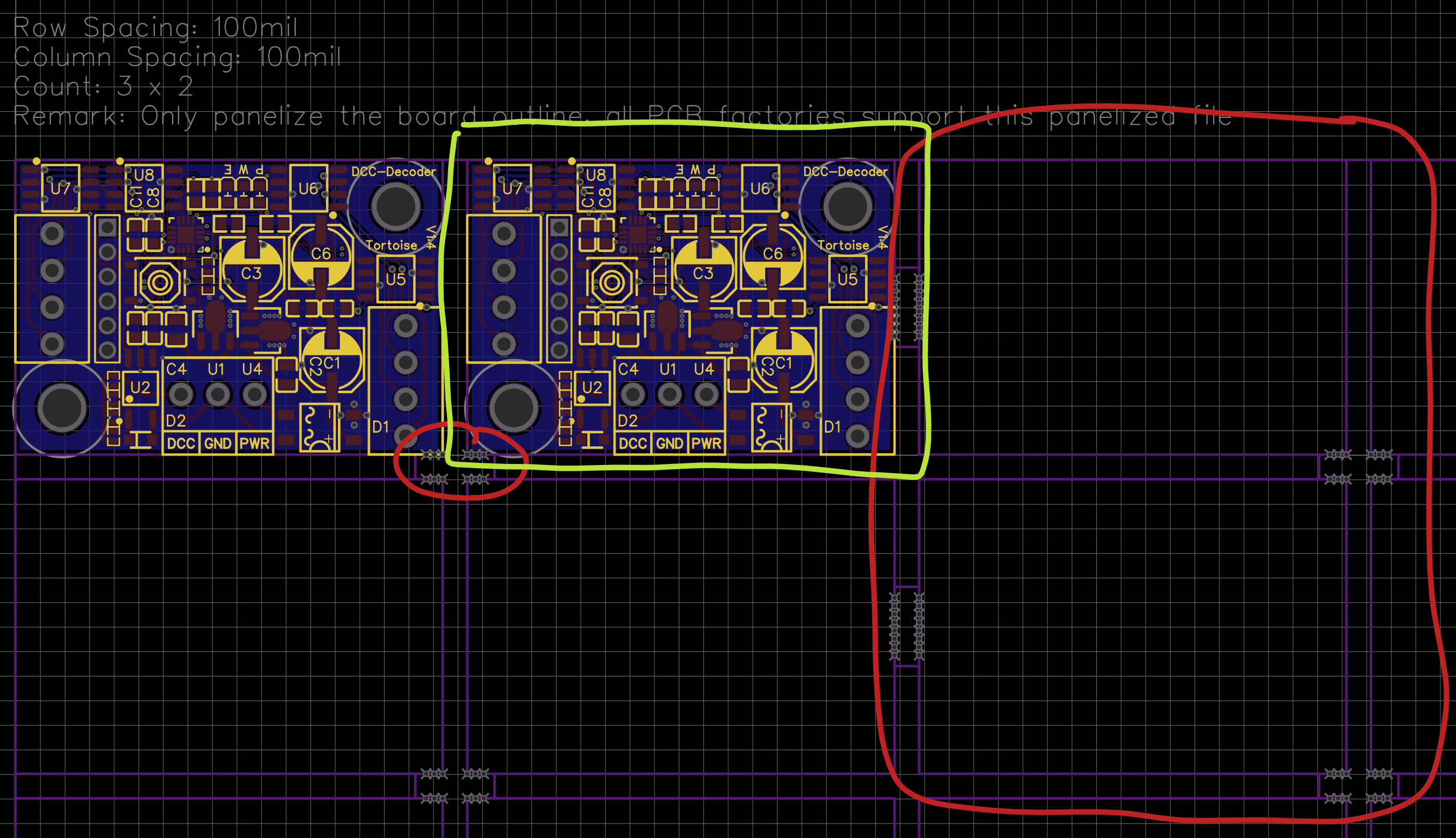
9\. Repeat as needed until all secondary boards are copied\. ![image.png](//image.easyeda.com/pullimage/spmfd1yBNc3Bxl9raqHzFZBDMhJEImymK8f26rPA.png) 
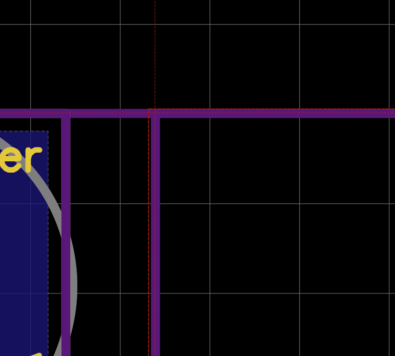
10\. Now we can fix the panelized outline\. For every secondary board\, select and delete the outline\. \(This will NOT delete/destroy the ground plane and is\, in essence\, why this guide works\!\) ![image.png](//image.easyeda.com/pullimage/7HJmmfUZwSdr2JVCkHyA8gGhmcX9HrckgyYsQMIC.png) 11\. Open the Panelize Dialog and set to "No Panelize"\. All of the purple lines should be removed except for the primary board outline\. This will clean up the outline mess that we made\. ![image.png](//image.easyeda.com/pullimage/NP5TBg2V71e4oDCgUsFdSQ4j7j4np2NksvJcpea9.png) 12\. Then re\-enable panelization\, with the exact same settings as before\. ![image.png](//image.easyeda.com/pullimage/5huRbNfpxx77I6Mg8yaM145kexrYMsRHPf1PWdaT.png) 
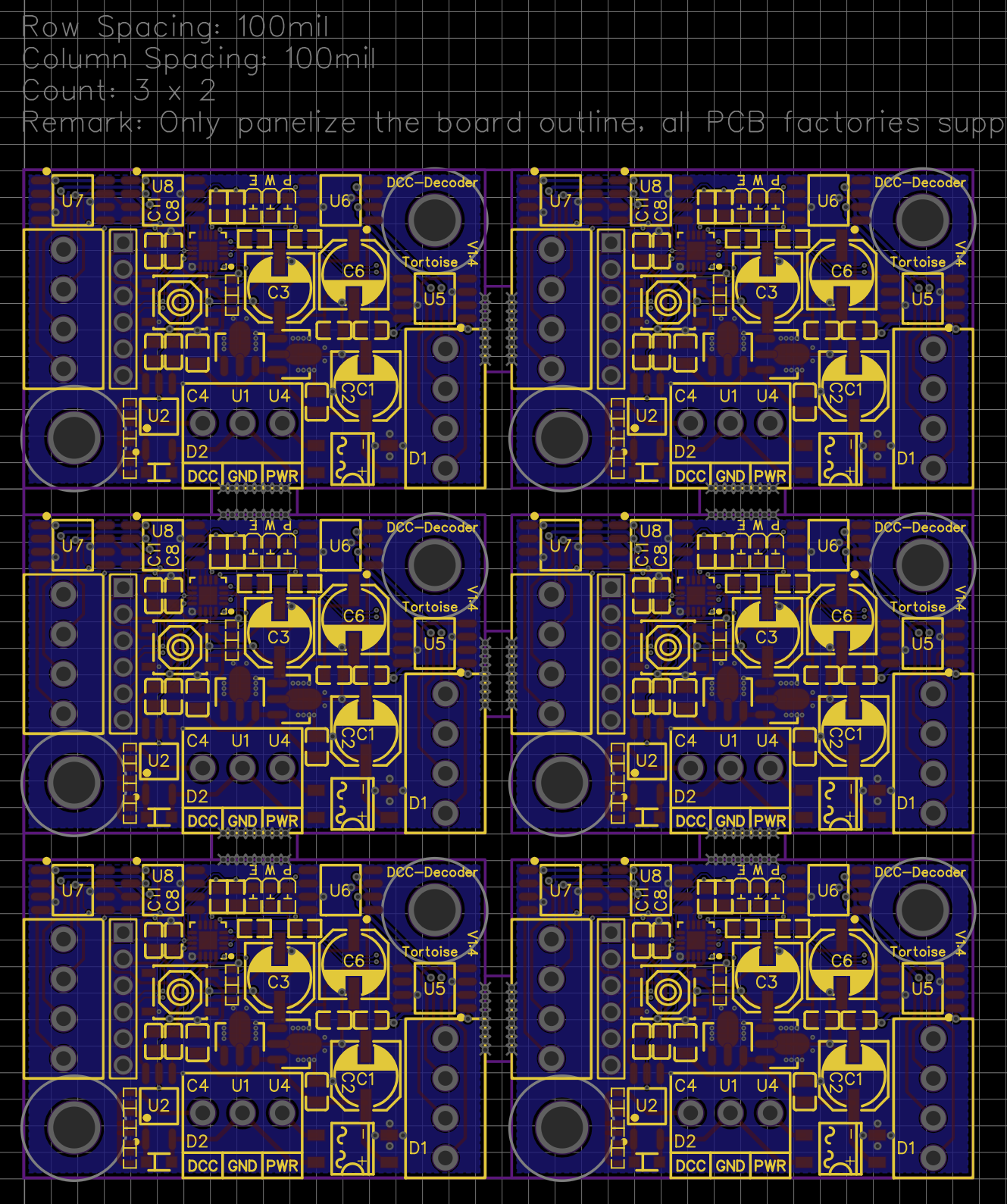
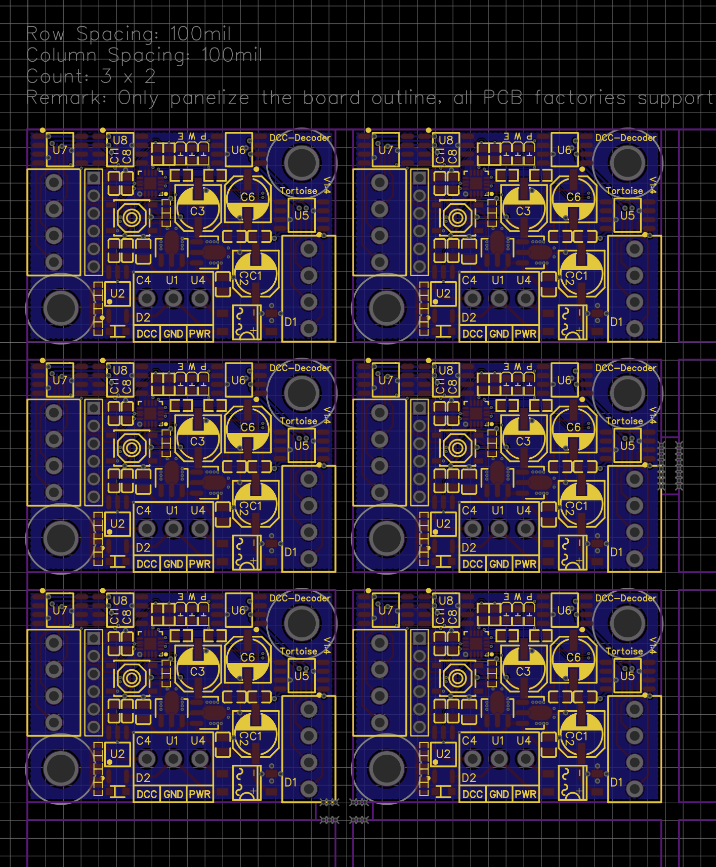
13\. You should now have a panelized board that a\) includes all components and layout on all sub\-boards b\) includes the ground plane for all sub boards and c\) has the correct outline for you panel\, including stamp holes\. You can generate gerber files for the panel and upload to JLCPCB\.
Comments
JLCPCBsupport 3 years ago
Well done !!
Reply
xpixer 3 years ago
Hello JLCPCB Support, instead of writing "Well done !!!" **you should at least fix this panellize function**!!! It can't be that the customers have to write a workaround just because you are not able to provide the function properly ... the least I expect is that this post will be linked in your FAQ.
Reply
JLCPCBsupport 3 years ago
@xpixer Tottaly understand. We will consider your request and we will add the post to the feature request category to be handled ASAP.
Reply
xpixer 3 years ago
Please check this, i demonstrate this Tutorial  :) [https://www.youtube.com/watch?v=GIxAq0j_has](https://www.youtube.com/watch?v=GIxAq0j_has)
Reply
Kai Chun Chou 3 years ago
What about the BOM and CPL files? Do we need to manually update the BOM?
Reply
bartpcb 3 years ago
Looks like CPL is based on the PCB and thus is automatically updated, the bom quantities should be updated manually it seems
Reply
andreacala 3 years ago
'morning, I tried to panelize by following these instruction but I've got 2 errors: 1) new elastics are created after 'paste ' command 2) the 'frame' or 'panel' after every 'paste' command is 'expanding' as in attached image. I've started from a matrix of 3 x 4 PCB and now the matrix has multiplied the number of PCB See the screenshot of what's has happened by redoing it twice. Where I'm wrong ? Thanks Andrea![Cattura1.JPG](//image.easyeda.com/pullimage/Ht2MP2pDzf1FK9PlNlo4q2GRbkNbRxvpxM6vN6La.jpeg)![Cattura2.JPG](//image.easyeda.com/pullimage/21ZSjYaHgcz4RUXfxs5Ajx6XsP02bKPgEyDpKkZd.jpeg)
Reply
andreacala 3 years ago
Hi, I've discovered why I was getting undesiderable 'elastic' as shown here above: because I was using  Opera  that didn't allowed me to do correctly the command CTRL+SHIFT+V.(past the copied objects) Unfortunately by changing browser and following the instructions I was not able to delete correctly the outlines of panelization.. And I'm likely sure this will happen on most cases. So, it doesn't work. Or, even if it works, the question for the EASYEDA software team is: When an user choose for 'panelization', the box that appears ask you how many rows & column of PCB you wish to panelize.. Here is: the software should replicate (copy) the PCB in the number of columns and rows choosen. It should be much simplier for a software to do this....
Reply
andreacala 3 years ago
So, I agree with XPIXER user: "you should fix this panelization-non-panelizing.
Reply
Mr_HaleYa 3 years ago
The new update makes this method not work, like the user above stated.
Reply
JLCPCBsupport 3 years ago
@Mr_HaleYa If you are no longer able to create PCB Panel in EasyEDA then you can write a new topic in the "bug Reports" section :) About "JLCPCB panel production" the PCB panel is getting improved continously to suit the customers needs and our process is getting better step by step, all what you need is to create your PCB file then in the JLCPCB order page you set the "Delivery format" regarding your need.. The delivery format is the method in which you ask JLCPCB to produce and deliver your PCB design. **· Single PCB** - Your design as is. **· Panel by Customer** - The customer constructs his PCB panel and supplies the data accordingly. **· Panel by JLCPCB** - We construct your panel with v-cut according to your need. (We only provide panelizing service for PCBs with regular shapes like rectangle and circle. For PCBs of irregular shapes, you need to panelize by yourself.) ![panel.JPG](//image.easyeda.com/pullimage/fTQQVaWzEqvK0a1eTeQKDs193p4ZXpCdZcSq6aoZ.jpeg)
Reply
Tone Electronix 3 years ago
This is frustrating. I have been exchanging emails with easyEDA support (and sometimes it's JLCPCB suport that answers me too...what a mess) and I can't figure out how to panelize a simple board with smt assembly - i mean a 3x4 panel with 3 smt components in each little board. Last email they said I should follow this topic/tutorial - what the hell, don't they have a proper how-to step-by-step on this operation, they need to refer to users good-will topics on a forum? So, as I said I tried all and, not surprisingly, I get all the issues that user @andreacala was having: ratlines all over the place, doubling outlines on the matrix. This is NOT a browser problem, since I am using the latest EasyEDA v6.4.7 windows software. FRUSTRATING! I guess it's time to move on for another pcb service provider.
Reply
JLCPCBsupport 3 years ago
@tone.electronix Hello ; About the SMT Assembly panel it should be panelized using stamp-holes because V-cut is not supported by our assembly service. About the design itself, it depends on the design tool that your are using, you can duplicate the design in one layout and create your panel using the duplicated design and you can create stamp-holes as drills respecting our production capabilities (min drill hole size and min drill hole clearance). You can find more details about our capabilities in the following link : [https://jlcpcb.com/capabilities/Capabilities](https://jlcpcb.com/capabilities/Capabilities)
Reply
Tone Electronix 3 years ago
@JLCPCBsupport The design tool I am using is EasyPCB. I did all that you mentioned (v-holes, duplication, rule check...). I was even pointed to this topic by your own email support, for a step-by-step instructions on how to panelize successfully. **Nothing worked**. And I must say this: JLCPCB/EasyEDA email support always missed the point, the issue. The problem is the design tool itself, EasyEDA software. You can see that even in this tutorial: the original post states it's  "Based on at least one EasyEDA hack/bug"! What kind of software "needs" a bug/hack to work as expected?! Shouldn't this process be easier enough for anyone trying to panelize with smt assembly??? Again, one word: FRUSTRATING
Reply
JLCPCBsupport 3 years ago
@tone.electronix Accidents could eventually occur but solving it is the key so we are trying to help you here to find a way out. "JLCPCB/EasyEDA email support always missed the point, the issue." Could you please tell us what is the main issue related to your order! You already said "**Nothing worked**. And I.." please can you share the design files so we can check it with you and since you already have produced the design can you share the images of the PCBs that you have received, this will help us to define the issue. Before placing the order you can check the design view using our Gerber viewer to check the final view of the production files.
Reply
Tone Electronix 3 years ago
@JLCPCBsupport Let's try again: Here's a small video of the issues I have trying to panelize: [https://youtu.be/_IGfAAlE7Mc](https://youtu.be/_IGfAAlE7Mc) And here's the project link with all the files included (BOM, gerbers, PnPlace) [https://easyeda.com/tone.electronix/3pdt-breakout-pcb](https://easyeda.com/tone.electronix/3pdt-breakout-pcb)
Reply
JLCPCBsupport 3 years ago
@tone.electronix Thank you for sharing all these details. Considering the video that you have posted, you better check again the step 6 of the guide "6. Use Ctrl+Shitf+C to copy by reference point. Use the upper left corner as reference point. Make sure you hit the corner of the primary board outline exactly, zoom in as needed." If you are properly coping the reference board than you will get the copper areas copied in the cloned boards as it mentions step 8 : "If everything is done correctly\, all of the primary board including the copper area is copied\. Note that since we enabled penalization \*and\* we also copied the outline of the primary board\, the panelization will be extended and look wrong\. We will fix this later\. \(Copying outline in this step is \*required\* because otherwise the copper area will not copy correctly\!\)" Considering step 8 it is normal to have extended boards every time you past a new clone board and it is mentioned to just ignore this because it will be removed once you re-create the panel as mentioned in step 12 : "Then re-enable panelization, with the exact same settings as before." Please make more try and let us know if you still encountering the same difficulty in coping the reference board with its copper area to the other cells. Please note that the project link has a PCB design file which supposed to be the panel file but it has only one PCB board design which is the reference board so kindly create your panel in it and we will help in investigating the design.
Reply
Tone Electronix 3 years ago
@JLCPCBsupport I adjusted the PCB Outlines, and alsoi tried my best to use ctrl-shift-c/v, zoomed in to get the best possible point for reference according to point 6.. Still, I can't get a copy WITH copper fill area as it should be according to point 8. And the ratlines are still present. I have updated the files on the project, also with gerber file for the panel. Please take a look. Thank you
Reply
Tone Electronix 3 years ago
@JLCPCBsupport Any news?
Reply
JLCPCBsupport 3 years ago
@tone.electronix tried many time but with no luck to copy the copper area, but I tried to recreate the copper area to all copied pieces and it works fine.
Reply
James Sleeman 3 years ago
After doing the CTRL-SHIFT-V to paste by reference the design, but **before** you delete the extra board outlines, you need to rebuild the copper pours with **SHIFT-B** this will repour all the pasted pours, then you can delete the board outlines (if you do this first then the pours will not pour).
Reply
James Sleeman 3 years ago
What I can't find out is if this is regarded as "Delivery Format: Single PCB" or "Delivery Format: Panel by Customer"? I note also that the gerber preview  does not show the cuts - might be preview bug? \-\-\- ![29.jpg](//image.easyeda.com/pullimage/gifZIjp9vdeEvNeuAgzZ10ppNRiXxHU5pHtbKYAX.jpeg) ![30.jpg](//image.easyeda.com/pullimage/21xhcqWxb9J4feT0GmrLeAhpH8Nqo0JCVBzLhn7z.jpeg) ![30.jpg](//image.easyeda.com/pullimage/m7OQ0h7z4xGaRgLgS1ZCmVMKH6ch5c9xPhHg6kMn.jpeg)
Reply
James Sleeman 3 years ago
Or maybe we can just use normal Panelize now, without this process and choose "Panelize by Customer" is that what it means?  Very confusing, JLC and EasyEda should make process much more clarified what exactly Panel by Customer means. ![P-10.jpg](//image.easyeda.com/pullimage/PRTzw6k5QlveercwCuiscAn0NkcU164CAeUfaRqB.jpeg)
Reply
JLCPCBsupport 3 years ago
@bitsyboffin Hello Thank you for the time taken to write for us here. About the ""Delivery Format: Single PCB" or "Delivery Format: Panel by Customer"?" That is considered as Panel by customer which is when you make your own panel (duplicated design in one board) and upload the GERBER to our ordering page, about the other option "**Panel by JLCPCB**" the GERBER must be a single PCB design and our engineers will create the panel depending on the setup of the "**Panel Format**" About how to properly create a PCB Panel please follow these rules : 1\. The V\-cut line should be the same as the outline of the Sub\-PCB\. That is to say\, there is zero space between the sub\-boards\. 2\. The V\-cut line can only be a vertical or horizontal straight line\. 3. The panel size of sample needs to be 70*70mm at least to do v-cut process. The longest edge  can not exceed 400mm, while the width  needs to be 70mm at least.4. The V-cut line must cross the whole panel or else the factory can't add a V-groove on the PCB because the milling cutter may destroy any sub-PCBs on the V-cut line. They also cannot stop part way across the panel. The V-cut lines shown below are not acceptable. ![](https://d33v4339jhl8k0.cloudfront.net/docs/assets/59f1de7804286313cffbb22c/images/5a17f100042863319924bbed/file-pXjAD3AZ3k.png) 5\. The maximum panel size with 0\.6mm board thickness is 100x100mm\. 6\. The maximum panel size with 0\.8\-1\.2mm board thickness is 200x200mm\.\(It will lead to more X\-out in a panel\, and has the risk of board twist and broken off if the size of the panel size is too large\.\) 7\. The maximum panel size with 1\.6mm board thickness is 300x300mm\. 8\. If you select the Edge Rails\, the MARK and Positioning Holes will be added to the Edge Rails default\, and local Fiducial Mark will not be added\. If the panel is provided already\, then no edges or Marks will be added again\. 9\. If there are more than 5 designs in one panel\, the panel size cannot exceed 200\*200mm\. Check the following link to learn more about it : [https://support.jlcpcb.com/article/49-pcb-panelization](https://support.jlcpcb.com/article/49-pcb-panelization)
Reply
James Sleeman 3 years ago
@JLCPCBSupport Why do you talk about v-cut when you can not do v-cut with assembly? We are talking here about making a Panel for **Assembly **in **EasyEDA** If I understand correct, if we make panel in EasyEDA "Panelize" option then we must choose "Panel By Customer", and that the blank area in panel that EasyEDA leaves will be filled in by JLC engineer?
Reply
Tone Electronix 3 years ago
@JLCPCBsupport > but I tried to recreate the copper area to all copied pieces and it works fine. What about the rat lines? Are they ok? Asking this because when I copy-paste they become an "extension" of the main board and gives a mess.
Reply
Tone Electronix 3 years ago
@JLCPCBsupport It turns like this mess: ![image.png](//image.easyeda.com/pullimage/P3Ojv5vzUlMv6RMF6fQvBXCtlNZbpsCfdvhKmJ0u.png)
Reply
JLCPCBsupport 3 years ago
@tone.electronix About the rat lines, this is an absolute EasyEDA subject and I tagged the support team in many comments to involve them in this discussion but it is better if you send an Email to [support@easyeda.com](mailto:support@easyeda.com) to get a better assistance @bitsyboffin Oh, you are right, I was talking as it is just a PCB panel not a PCB panel assembly. For Panel SMT Assembly V-cut is not supported and the panel should be made by stamp-holes. About your comment : " if we make panel in EasyEDA "Panelize" option then we must choose "Panel By Customer"" yes, whatever software you use for your PCB panel design, you choose the "Panel by Customer" if your design is already a panel, but if you want JLCPCB engineers to create the panel for you then just upload a single PCB design and it will be duplicated in panel.
Reply
adamalfath 3 years ago
I'm trying to panelize using this method but it introduce unwanted stamp hole position, in my case it is in the castellated hole area. How can I deal with this? I try to create my own panel outline (free draw, not generated panel) but the gerber failed to show at JLC order page. Panelize using method explained above: ![panel.png](//image.easyeda.com/pullimage/RVpeeHLVoTq63so6foVVRQylyb2V7MfdDsrwPfLv.png) Free draw panel (JLC fail to load the gerber, dimension unknown): ![panel.jpg](//image.easyeda.com/pullimage/eKYUI9z0xr7ECI4n2RfE3yc9FBB3aWzTtHZTJVqP.jpeg)
Reply
JLCPCBsupport 3 years ago
@adamalfath Hello :) Thank you for the time taken to write your comment here. A panel can't be created without the stamp holes in the ROWs (minimum Hole group is 1) technically your design has a castellated edge all along the board sides, I suggest you to create a column panel instead of a Row panel but in this case you won't be able to create panel boarder. The following image shows the panel settings that could help you to solve the issue. ![panel.JPG](//image.easyeda.com/pullimage/ekJlDcgFSYtvxEUgPpfmOF3WEF2cUw8JCtlwE2Ot.jpeg)
Reply
Aivan 3 years ago
I got fed up with this, I just used this instead [https://github.com/ThisIsNotRocketScience/GerberTools](https://github.com/ThisIsNotRocketScience/GerberTools)
Reply
david.knell 3 years ago
I got fed up with this too, so I wrote [https://github.com/pifi-bz/easyeda-panel](https://github.com/pifi-bz/easyeda-panel) \- and now it appears that JLCPCB will accept a 'panelized' file from EasyEDA and sort everything out for you\.  Which\, to be honest\, is how it should be\.
Reply
Raonari 3 years ago
I lost via after copy the pcb. ![화면 캡처 2020-12-15 033727.png](//image.easyeda.com/pullimage/5XEifamoeMdMJDsESLdTp2P3wB7PYOVQtXFFgOxN.png) Thus, I waste 60 PCB with SMT (about $500) !!! Of course, it is my responsibility for not checking! But, Why JLCPCB recommended EasyEDA? We are not B-tester! EasyEDA should be more reliable.
Reply
JLCPCBsupport 3 years ago
Hello all ; Maybe this is the first time a similar thing happened with EasyEDA. @[andyfierman](https://easyeda.com/andyfierman) [@](https://easyeda.com/andyfierman)[UserSupport](https://easyeda.com/UserSupport)<br> <br>
Reply
Tommaso Sabìa 2 years ago
@david.knell Hi, what do you mean EXACTLY by "they sort everything out for you"? After exporting a Panelized version from EasyEDA, do we also need to select "Panel by customer" during the JLCPCB order? Or do we just keep it on "Single PCB" and everything will work by itself?
Reply
Jaga 2 years ago
Also interested in that. What is the proper panelizing process currently? Thanks.
Reply
Tommaso Sabìa 2 years ago
@david.knell no response yet :(
Reply
lqhuy2205 4 months ago
@tommaso.sabia did you try it yet ?
Reply
Login or Register to add a comment
goToTop
你现在访问的是EasyEDA海外版,使用建立访问速度更快的国内版 https://lceda.cn(需要重新注册)
如果需要转移工程请在个人中心 - 工程 - 工程高级设置 - 下载工程,下载后在https://lceda.cn/editor 打开保存即可。
有问题联系QQ 3001956291 不再提醒
svg-battery svg-battery-wifi svg-books svg-more svg-paste svg-pencil svg-plant svg-ruler svg-share svg-user svg-logo-cn svg-double-arrow -mockplus- -mockplus- -mockplus- -mockplus- -mockplus- -mockplus- -mockplus- -mockplus-@1x -mockplus-

Cookie Notice

Our website uses essential cookies to help us ensure that it is working as expected, and uses optional analytics cookies to offer you a better browsing experience. To find out more, read our Cookie Notice