You need to use EasyEDA editor to create some projects before publishing
How thick is the through-plating of a through hole pad?
6391 10
Luks 5 years ago
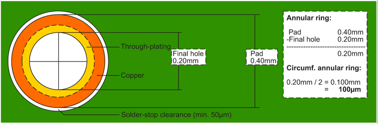
Hello, I would like to implement a press-fit contact. The manufacturer describes the requirements of the pad very accurate, as you see below. ![Pad_AnnularRing_Copper.jpg](//image.easyeda.com/pullimage/ZFNj1gNtLSEXEKOLYgv8t48GCImzfPN4s5FPGjES.jpeg) I want my design to suit the description but I don't know where to set the through-plating thickness. ![image](https://www.multi-circuit-boards.eu/fileadmin/img/03_Design-Hilfe/restring/pcb_annular-ring_standard.gif) Thanks in advance and best regards, Lukas
Comments
andyfierman 5 years ago
@Luks, Please see: [https://jlcpcb.com/capabilities/Capabilities](https://jlcpcb.com/capabilities/Capabilities) and repost this in the JLCPCB section of the forum. Note also this post: [https://easyeda.com/forum/topic/Hole-size-tolerance-for-Holtites-868f5c9d3eba41d79065fef7479a6248](https://easyeda.com/forum/topic/Hole-size-tolerance-for-Holtites-868f5c9d3eba41d79065fef7479a6248) Thanks.
Reply
Luks 5 years ago
@andyfierman Thanks you for the fast response, Andy. But I can't find an answer to my question under the website from JLC and the post of Fred Wright also does not help. I spent a lot of time in the forum today and didn't find an answer, thats why I created this post. I would be grateful if you could give me further information.
Reply
andyfierman 5 years ago
@Luks, Your question is answered because part of the Wuerth Elektronic ICS - Press Fit Specification 5.1 requires a **hole diameter tolerance of +/-0.025mm** but on the JLCPCB Capabilities page it says: | | | | --- | --- | | Hole Size Tolerance | ±0.08mm | which exceeds the Wuerth specification. You have said: "I want my design to suit the description " but the above figures show that you cannot, so asking about the through hole plating thickness is actually irrelevant. If however, you still want to know the through hole plating thickness then you can ask directly by email to support at JLCPCB.com
Reply
Luks 5 years ago
@andyfierman The actual question of the post was "How thick is the through-plating of a through hole pad?". So it is not irrelevant. Besides other users might ask themselve the same question an then they could find the answer here.
Reply
andyfierman 5 years ago
@Luks, Yes you asked how thick the through plating was but you then went on to describe that: "I would like to implement a press-fit contact. The manufacturer describes the requirements of the pad very accurate..." and then presented the spec for doing so. That spec includes a requirement for the hole diameter which JLCPCBs standard processes cannot meet so therefore you cannot reliably use your preferred press-fit contacts. Therefore in this context there is little point in knowing the through plating thickness when another parameter in the PCB process will prevent you from using them anyway. I recognised that there may be other reasons that you may wish to know the through hole plating thickness but (a) I do not know the value and (b) I do not work for JLCPCB which is why I then went on to say that: "If however, you still want to know the through hole plating thickness then you can ask directly by email to support at JLCPCB.com". Regarding your concern that: "Besides other users might ask themselve the same question an then they could find the answer here.", if you get an answer from JLCPCB on this then it would be very helpful to others if you post it back here for anyone to see.
Reply
Luks 5 years ago
I got an answer from JLCPCB. The thickness of the copper plating is 18 µm. ![Through plating.jpg](//image.easyeda.com/pullimage/LMyr9ChxkPkQejL3GwEihSRZXclPsBvFFGGPhEdZ.jpeg) I also found out that the minimum hole size of a plated through hole pad is 0.65 mm and the maximum hole size is 6.3 mm.
Reply
andyfierman 5 years ago
@Luks, Thanks for posting this information back to the forum. :)
Reply
LISA_DALTON 4 years ago
[andyfierman](https://easyeda.com/andyfierman) & @Luks, I was just wondering the same thing about the PTH copper thickness. @ .18um, it is not too significant. -Lisa Dalton.
Reply
andyfierman 4 years ago
I am still waiting for JLCPCB to answer some more specific questions: [https://easyeda.com/forum/topic/Questions-about-the-dimensions-of-two-adjacent-multilayer-PTH-pads-137d9c147a3649bd9adcf52e9a29899b](https://easyeda.com/forum/topic/Questions-about-the-dimensions-of-two-adjacent-multilayer-PTH-pads-137d9c147a3649bd9adcf52e9a29899b)
Reply
MikeDB 4 years ago
18 um is worryingly thin.  I thought the industry standard was 25um.  This means all vias have 50% more resistance than you thought they had.
Reply
Login or Register to add a comment
goToTop
你现在访问的是EasyEDA海外版,使用建立访问速度更快的国内版 https://lceda.cn(需要重新注册)
如果需要转移工程请在个人中心 - 工程 - 工程高级设置 - 下载工程,下载后在https://lceda.cn/editor 打开保存即可。
有问题联系QQ 3001956291 不再提醒
svg-battery svg-battery-wifi svg-books svg-more svg-paste svg-pencil svg-plant svg-ruler svg-share svg-user svg-logo-cn svg-double-arrow -mockplus- -mockplus- -mockplus- -mockplus- -mockplus- -mockplus- -mockplus- -mockplus-@1x -mockplus-

Cookie Notice

Our website uses essential cookies to help us ensure that it is working as expected, and uses optional analytics cookies to offer you a better browsing experience. To find out more, read our Cookie Notice