I keep getting objects in Gerber files that are not in PCB designs.
Some can be deleted in gerbers (though remain when creating new Gerbers)
Some cannot be deleted in Gerber and remain in Photo version, but cannot be found in PCB design.
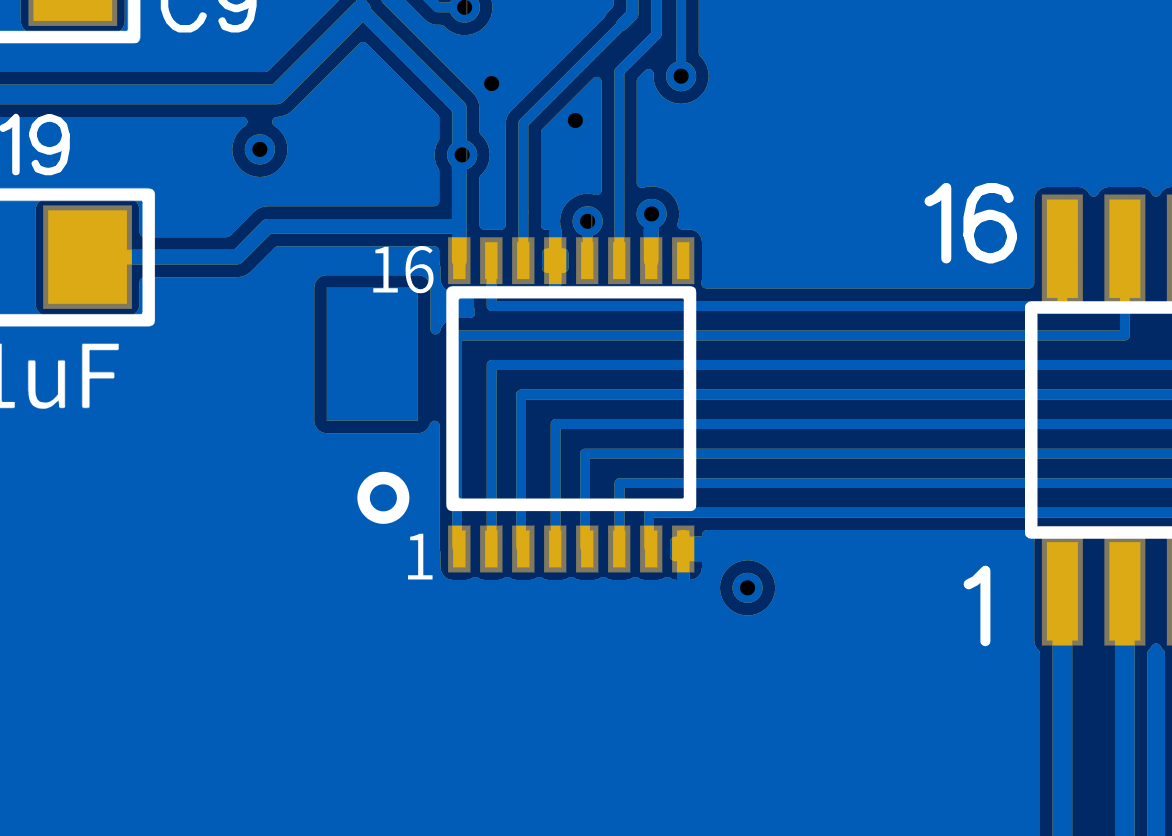
@andyfierman Here is a bottom silk shot and the bottom image.
Note circles on omage are not on bottom silk or any other layer.
I have others , but this is the sort of issue I've been having.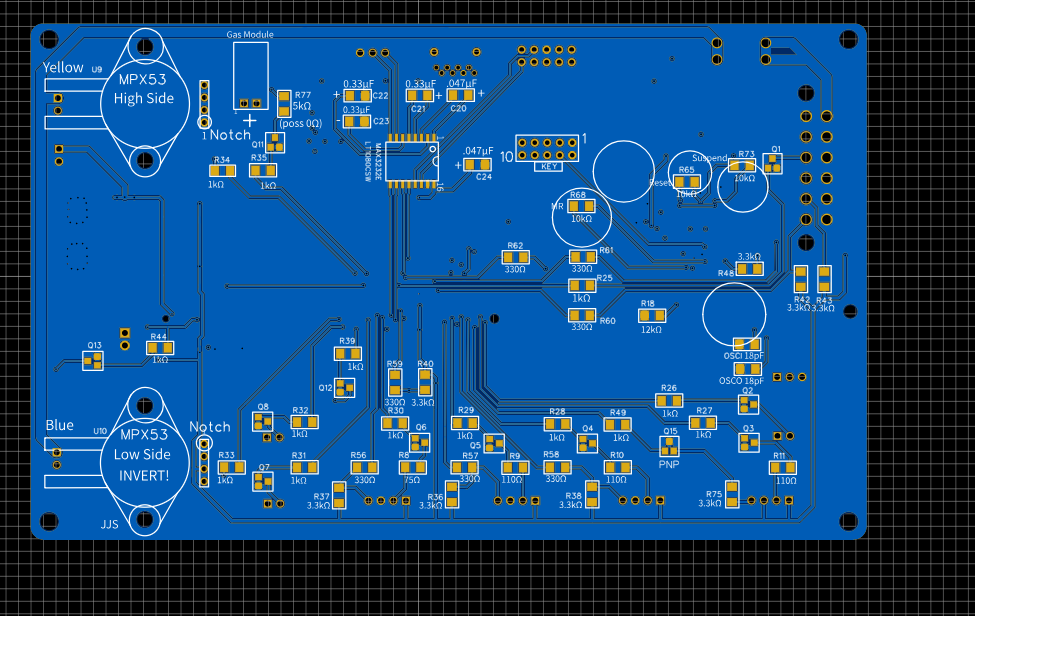
There are a few others.
One having to do with NOT deleting solder mask when deleting traces ruined a batch of what I call Power Modules.
The issue was not visible in PCB design, but showed up on PCBs when delivered.
These appear in Gerbers, but deleting them there do not change the fact they are still in PCB layers, but cannot be seen in EASY PCB.
The main problem is that I can correct these issues in Gerbers, but should I later make a small change in design the error is not visible in design,but shows up in PCBs ordered.
I should not have to keep correcting same issues in Gerbers for every revision in design when those issues are not visible.
It must be a basic flaw in your "Delete" process, because it's no longer visible, but still there somewhere.
To restate: not all of an object is actually deleted, but it appears to have been in design layers, then still shows up in Photo Image and Gerbers.
At first I thought it was just a problem in your photo process, but was wrong. It persists somewhere in memory, but not on any layer.
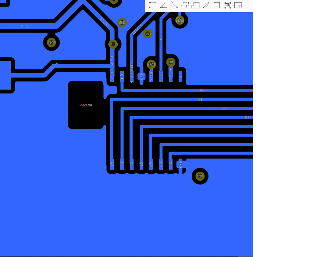
@andyfierman Here is another one where Pwren is of "visible" Top layer. See blank rectangle with " Pwren" in it. I think this may have something to do with it. The next is a photo view. That rectangle seems to be a trace.
I had a trace in this layer, but deleted it a few versions ago. This blank remains here, but on Photo and PCB it is filled in as it appears in Photo view.
Again can delete in Gerber, cannot find in any layer, remains in next Gerber build.
This actually presents no functional issue, but points to the issue I'm having.
Our website uses essential cookies to help us ensure that it is working as expected, and uses optional analytics cookies to offer you a better browsing experience. To find out more, read our Cookie Notice


 Brand new interactions and interfaces.


 Easy to use and quick to get started.