You need to use EasyEDA editor to create some projects before publishing
Please verify my AC driver circuit using OPTO & TRIAC
2578 17
aledrus 3 years ago
Hi 
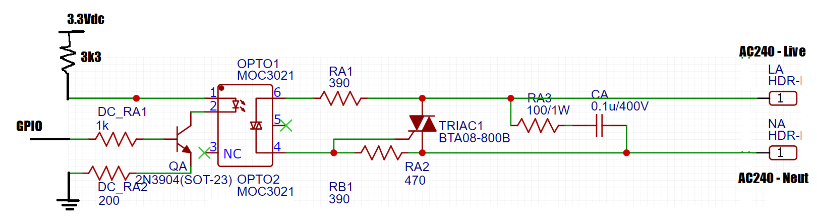
As I've introduced myself in the previous post, I am quite new at this. I have some experience with using relays to drive an AC load, but here I want to not use 5V or 12V altogether. So I recently discovered that I could use an optotriac + triac combo to drive a load like a relay. I need someone who has more experience to teach me if I've done something wrong here and if so, what did I miss? GPIO signal is a 0/3.3V signal. This is to drive an inductive/resistive load. (I built this circuit using a breadboard without the AC connected. With a multimeter on the AC pads, I measured infinite ohms when GPIO is low and about 12 MOhms when GPIO is high. I am expecting 0 ohms when GPIO is high, like a relay would - but as I understand the triac resistance depends on the current going through. Anyway, I am not confident with this circuit because of this) Thank you in advance! ![AC load driver with triac](//image.easyeda.com/pullimage/4xjPAvqBa1hGNLHWhhZ6rTsKsUlpH83CbRyMH3DD.png)
Comments
andyfierman 3 years ago
First question is: Where's your Design Requirements Specification? Without that no-one knows for sure what your requirements are here. AC voltage to be switched (240V is that RMS/Peak)? AC frequency (50Hz/60Hz/400Hz)? Load current to be switched?
Reply
aledrus 3 years ago
I don't have a design requirement specification. I'm just trying to control some home lights and fan. AC voltage is 230V 50 Hz Load current varies for different lights wattage up to 100W, and for fan it is less than 100W
Reply
andyfierman 3 years ago
Please check the device datasheet and apps notes: [https://www.onsemi.com/pdf/datasheet/moc3023m-d.pdf](https://www.onsemi.com/pdf/datasheet/moc3023m-d.pdf)<br> <br> [https://www.onsemi.com/pub/collateral/an-3003.pdf](https://www.onsemi.com/pub/collateral/an-3003.pdf)<br> <br> The MOC3021 is specified for 240V mains so you can ignore Fig 7.
Reply
andyfierman 3 years ago
Why not try connecting a bench supply set to say 30V with a 1A current limit across the AC terminals in either polarities and see if you can short out the PSU by turning your triac on and off?
Reply
eichenlaubl 3 years ago
@aledrus I am not familiar with the triac but can offer some advice on your drive circuit. I believe it will function as designed. However it is more complex than necessary. You can discard Ra1 Ra2 and Qa. Connect GPIO to pin 2 of the opto isolator. This will reverse the on/off states from your original design. To keep the on/off states the same, connect the 3.3K from pin 2 to ground and connect GPIO to pin 1. <br> <br> <br> <br> <br> <br>
Reply
eichenlaubl 3 years ago
@eichenlaubl I took a look at the data sheet and realized neither your original drive circuit or my simplified version is adequate as they provide less than 1ma current and more than 10 ma is required. If you let me know what you are providing GPIUO with I will design in driver for you.
Reply
andyfierman 3 years ago
@aledrus, Note (2) in the MOC30xx datasheet states: "All devices are guaranteed to trigger at an IF value less than or equal to max IFT. Therefore, recommended operating IF lies between max IFT (30 mA for MOC3020M, 15 mA for MOC3010M and MOC3021M, 10 mA for MOC3011M and MOC3022M, 5 mA for MOC3012M and MOC3023M) and absolute maximum IF (60 mA)." Therefore you should design for an IF of something like (15mA+60mA)/2 = 37.5mA, say between 35mA and 40mA. Looking at **Figure 2. LED Forward Voltage vs. Forward Current** in the datasheet, if you: 1. connect QA emitter directly to ground; 2. increase DC_RA1 to (3.3V-0.6V)/1mA = 2.4k;  3. reduce the 3.3k resistor to (3.3V-1.5V)/36mA = 48 Ohms, so choose 47 Ohms then that will drive almost exactly 35mA through the LED in the MOC3021, requiring a current from GPIO into the base of QA of about 1mA. However this is a very power hungry solution requiring 3.3V*(1mA+35mA) = 118.8mW just to turn the triac on. This also means that there will be a step change in 3.3V supply current of 36mA every time the triac is turned on or off. This will require additional 3.3V rail decoupling of between 10uF to 100uF, placed across the top end of the 47 Ohm resistor to ground at the emitter of QA. Although this may not be a problem if the 3.3V supply is well regulated, the design is also poor from the point of view of regulation of IF. With a series resistor of 47 Ohms any change in the 3.3V supply voltage will produce a large swing in the LED current. You could design for a working IF of say 23mA (series resistance of about 75 Ohm) but probably not much lower since the LED forward drop will increase at lower temperatures and so may limit the lower end IF achievable. You would be better to use the MOC3023 with its max IF of 5mA and design for a working IF of say 15mA. For the components around the mains side of the MOC302x  please refer to Figure 12. Typical Application Circuit in the datasheet for recommendations. Note that the 0.05uF cap could be reduced to 0.047uF. The load of course can be placed in either the "HOT" or "GROUND" side which in your case correspond to Live and Neutral. * Your project is private so only you can see it. * You have prefixes for two resistors RA2 and RB1. It is not clear which resistor in your screenshot that these prefixes and values refer to. * The resistor from A1 to Gate of the triac appears to be unnecessary. Please check Fig 14 in: [https://www.st.com/resource/en/application_note/dm00096037-how-to-select-the-triac-acs-or-acst-that-fits-your-application-stmicroelectronics.pdf](https://www.st.com/resource/en/application_note/dm00096037-how-to-select-the-triac-acs-or-acst-that-fits-your-application-stmicroelectronics.pdf)<br> <br> and the other documentation in: [https://www.st.com/content/st_com/en/products/thyristors-scr-and-ac-switches/triacs/standard-and-snubberless-triacs/bta08.html#documentation](https://www.st.com/content/st_com/en/products/thyristors-scr-and-ac-switches/triacs/standard-and-snubberless-triacs/bta08.html#documentation)<br> <br>
Reply
aledrus 3 years ago
Hi both. Thank you very much for your replies. I have been trying to digest what you've written and I'm slowly getting there. @[eichenlaubl](https://easyeda.com/eichenlaubl) The device that is supplying the GPIO signal is an ESP8266. I read somewhere that it is not enough to turn the LED on because its internal resistors are too weak or not large enough to drive enough current. I think these two statements are contradicting but maybe I'm wrong, so I've added that NPN transistor (QA) to rule it out. @[andyfierman](https://easyeda.com/andyfierman) that is a very detailed reply and I think you so much for it. I don't quite grasp it all yet though but I'll get there. A few items, I don't currently have a 30Vac supply so I won't be able test that. As per your comments about the AC driver design: "trigger at an IF value less than or equal to max IFT"  - for the MOC3021 the max IFT is 15 mA and recommended IF should be between 15 mA and 60 mA. Why do you recommend 37.5 mA instead of say, 16mA (15 mA max IFT + 1 mA)? "increase DC_RA1 to (3.3V-0.6V)/1mA = 2.4k;"  - Can you show me where I can find the source for the 1 mA? Please bare with me I did read through the datasheet but I am not very familiar with the structure of the document yet, so I cannot truly say that I read it all. I truly appreciate when you went on to say Figure X in doc Y in the rest of your response because that truly helped me find relevant material in the documentation. "reduce the 3.3k resistor to (3.3V-1.5V)/36mA" - Similarly, how was the 1.5V determined? "This also means that there will be a step change in 3.3V supply current of 36mA every time the triac is turned on or off. This will require additional 3.3V rail decoupling of between 10uF to 100uF, placed across the top end of the 47 Ohm resistor to ground at the emitter of QA. Although this may not be a problem if the 3.3V supply is well regulated, the design is also poor from the point of view of regulation of IF. With a series resistor of 47 Ohms any change in the 3.3V supply voltage will produce a large swing in the LED current."  - This part when over my head and I think I may need to read other more introductory material to understand what this means. "but probably not much lower since the LED forward drop will increase at lower temperatures and so may limit the lower end IF achievable." - if the device is guaranteed to trigger at IF value of less than max IFT, should it be possible to trigger at 14 mA (if max IFT is 15 mA?) "the 0.05uF cap could be reduced to 0.047uF" - could you help me understand how the 0.047 uF figure is determined? Is it because 0.05 uF doesn't exist in the market but 0.047 uF does? "You have prefixes for two resistors RA2 and RB1" - Sorry, please ignore the RB1. That resistor is RA2. Looking at the Typical Application Circuit in the MOC3023m datasheet (Fig 12), it looks like the mains side of my design is completely wrong/different. In the Typical Application Circuit, the MOC pin 4 is connected to the gate of the triac only. In mine above, MOC pin 4 is connected to both the gate and Terminal 2 of the triac. Is it true that even aftermy original design would definitely not work even if I remove the resistor from the gate? <br> Thanks all. I appreciate your experience and your writing to help.
Reply
andyfierman 3 years ago
@aledrus, "trigger at an IF value less than or equal to max IFT"  - for the MOC3021 the max IFT is 15 mA and recommended IF should be between 15 mA and 60 mA. Why do you recommend 37.5 mA instead of say, 16mA (15 mA max IFT + 1 mA)? Since your led drive is a low value resistor fed from a low voltage source, you have to allow for the resistor tolerance, the power supply tolerance, the driving transistor saturation voltage and the tolerance and temperature changes of the forward voltage drop of the IR LED. Plus, opto couplers have a tendency for the coupling between the LED and the opto receiver device to drop throughout their lifetime. So you need to allow a good margin. "increase DC_RA1 to (3.3V-0.6V)/1mA = 2.4k;"  - Can you show me where I can find the source for the 1 mA? Please bare with me I did read through the datasheet but I am not very familiar with the structure of the document yet, so I cannot truly say that I read it all. I truly appreciate when you went on to say Figure X in doc Y in the rest of your response because that truly helped me find relevant material in the documentation. The 0.6V is the typical forward Vbe drop of a bipolar transistor. A more rigorous anaylis would cover the corner cases of 0.55V to 0.7V or even wider if you cover an extended temperature range. "reduce the 3.3k resistor to (3.3V-1.5V)/36mA" - Similarly, how was the 1.5V determined? It's a compromise value for the max forward drop of the IR LED from careful reading of the MOC3021 datasheet: * VF Input Forward Voltage in the table of Electrical Characteristics, even at the quoted 10mA this could go as high as 1.5V also: * Figure 2. LED Forward Voltage vs. Forward Current and look up at about 36mA then allow some more for the maximum because these graphs are usually based around the typical values. "This also means that there will be a step change in 3.3V supply current of 36mA every time the triac is turned on or off. This will require additional 3.3V rail decoupling of between 10uF to 100uF, placed across the top end of the 47 Ohm resistor to ground at the emitter of QA. Although this may not be a problem if the 3.3V supply is well regulated, the design is also poor from the point of view of regulation of IF. With a series resistor of 47 Ohms any change in the 3.3V supply voltage will produce a large swing in the LED current."  - This part when over my head and I think I may need to read other more introductory material to understand what this means. The first bit is about power supply decoupling and the second part is simple Ohms law. Please read and play with the simulations in: [https://easyeda.com/forum/topic/UPDATED-Power-supply-decoupling-and-why-it-matters-30a39d0a77f34d5d8dc77e37c035b3d3](https://easyeda.com/forum/topic/UPDATED-Power-supply-decoupling-and-why-it-matters-30a39d0a77f34d5d8dc77e37c035b3d3)<br> <br> and: [https://easyeda\.com/andyfierman/LEDs\_must\_have\_series\_resistors\-OoGYgCK2k](https://easyeda.com/andyfierman/LEDs_must_have_series_resistors-OoGYgCK2k)<br> <br> "but probably not much lower since the LED forward drop will increase at lower temperatures and so may limit the lower end IF achievable." - if the device is guaranteed to trigger at IF value of less than max IFT, should it be possible to trigger at 14 mA (if max IFT is 15 mA?) Very good question! Short answer: absolutely not. Long answer: It's very badly worded in the datasheet. It seems nonsensical to say that "All devices are guaranteed to trigger at an IF value less than or equal to max IFT". That implies you could trigger them with zero current. The IFT max shown is actually the guaranteed worst case IFT required to trigger the device. The actual IF required may be lower than this but to guarantee triggering in all conditions, IF must be greater than or equal to IFT. What would be easier to understand is if the table showed that IFT is the MINIMUM LED current required to trigger. And therefore it should say that: "All devices are guaranteed to trigger at an IF value GREATER than or equal to max IFT". If you read note (2) in TRANSFER CHARACTERISTICS in the table of Electrical Characteristics and note the last sentence, it states that IF should be between IFT and IFAbsMax, which does, eventually, makes sense. "the 0.05uF cap could be reduced to 0.047uF" - could you help me understand how the 0.047 uF figure is determined? Is it because 0.05 uF doesn't exist in the market but 0.047 uF does? Pretty much. 0.05uF (50nF) may exist in the high voltage caps ranges intended for use as here, in snubber networks, but they are rare and therefore, expensive and at the moment probably made of Unobtainium. Some of the parts on offer are not suitable because they are not high enough voltage rated or have lousy Voltage Dependence of Capacitance or Voltage Coefficient of Capacitance (sometimes confusingly abbreviated to VDC or VCC) due to the dielectric materials used (but that's a whole new bag of parameters: [https://blog.knowlescapacitors.com/blog/test-parameters-and-electrical-properties](https://blog.knowlescapacitors.com/blog/test-parameters-and-electrical-properties)). Looking at the Typical Application Circuit in the MOC3023m datasheet (Fig 12), it looks like the mains side of my design is completely wrong/different. In the Typical Application Circuit, the MOC pin 4 is connected to the gate of the triac only. In mine above, MOC pin 4 is connected to both the gate and Terminal 2 of the triac. Is it true that even aftermy original design would definitely not work even if I remove the resistor from the gate? Your circuit is correct except that as I said: "The resistor from A1 to Gate of the triac appears to be unnecessary." That is your 470R resistor, RA2. Your circuit will work as intended with or without it but including it has little effect other than to make the triac less sensitive to false triggering at the expense of wasting a small amount of extra power when the gate drive to the triac is turned on. To understand why, you need to read up on exactly what: 1. a triac is and how it works: 1. [https://en.wikipedia.org/wiki/TRIAC](https://en.wikipedia.org/wiki/TRIAC); 2. [http://web.archive.org/web/20120107042632/http://www.onsemi.com/pub_link/Collateral/HBD855-D.PDF](http://web.archive.org/web/20120107042632/http://www.onsemi.com/pub_link/Collateral/HBD855-D.PDF); 2. the MOC3023 is doing in the circuit. These simulations will help you (one of which I'd forgotten about until just now!); [https://easyeda\.com/andyfierman/MOC3023M\_test\_jig\-33a999bae82f45e5b4a1300c4c5735b5](https://easyeda.com/andyfierman/MOC3023M_test_jig-33a999bae82f45e5b4a1300c4c5735b5)<br> <br> You could put a footprint for RA2 in the PCB but not populate it by setting the Convert to PCB=Yes and Add into BOM=No attributes for RA2. Except for RA2 which should only ever see a couple of volts across itself, you must use mains side resistors with a big enough spacing between the inside edges of their pads (or series combinations with a cumulative gap) to withstand the peak voltage of the mains and strictly, to meet the maximum voltages of the mains surge and fast transient burst tests: [https://www.nutwooduk.co.uk/archive/keitharmstrong/emc_testing3.html](https://www.nutwooduk.co.uk/archive/keitharmstrong/emc_testing3.html)<br> <br> [https://easyeda.com/forum/topic/Getting-Started-with-EMC-and-EM-Engineering-Some-useful-resources-Author-Keith-Armstrong-d9fdd474c221453da41cbd9d639cecd9](https://easyeda.com/forum/topic/Getting-Started-with-EMC-and-EM-Engineering-Some-useful-resources-Author-Keith-Armstrong-d9fdd474c221453da41cbd9d639cecd9)<br> <br> This pretty much rules out anything smaller than 1206 in SMT and even then you would need two or three in series to meet the clearance requirements.
Reply
andyfierman 3 years ago
@aledrus, "A few items, I don't currently have a 30Vac supply so I won't be able test that." Triacs are bidirectional (and almost symmetrical) so you only need a DC supply. :)
Reply
aledrus 2 years ago
@andyfierman Hi Andy! Thanks for your reply. I really thought I've replied to you but I think I must have postponed it until I managed to test it. I realise it's been months but real life got in the way. I've just built the circuit on a board, the schematic is as attached. ![eda.png](//image.easyeda.com/pullimage/KX8DxdCnNQNmWHKMV1pzlJzNURSxEMU65ES1ro7B.png) I took your advice and tried to design it for a working IF of 15 mA. I used R = (3.3V-1.5V) / 0.015A = 120 ohm for between VCC and Pin 1 of the MOC. I also forgot to add the 1mA from the base, but taking the Figure 2 LED Forward Voltage vs Forward Current at 16 mA should be about 1.4V voltage drop I figured the 1mA from the base is negligible (I hope that's right) The DC side (left) works to ground pin 2 of the MOC3023. Without load on the pad (AC1), the voltage switched from 0V to 230V as expected. When I put a load on the pad AC1 (I tried to supply an old 250W computer PSU), the 390R AC_RA1 blew up. I think it has something to do with it being an ordinary resistor rather than a higher wattage one. But in the datasheet (Figure 12 of [MOC3023M - 6-Pin DIP Random-Phase Triac Driver Output Optocoupler (250/400 V Peak) (onsemi.com)](https://www.onsemi.com/pdf/datasheet/moc3023m-d.pdf)) it does not specify what wattage of the resistors should be used. Do I need a special resistor? I thought it would be the TRIAC BTA08 that would be doing the AC switching rather than the MOC3023 itself (which I assume switches the TRIAC), so not much current would need to pass through AC_RA1 to cause it to blow. I am learning a bit more but I have just realised that I still don't know what's my problem.
Reply
aledrus 2 years ago
I don't know if this matters, but the little light on the power supply (image below) blinks when I try to supply RA2 (base of the NPN BJT) a 3.3V from the power supply. The 3.3V supplies both RA1 and RA2. It's fine when RA2 is disconnected. I think it means there is a short/fault/overcurrent in the system but all it supposedly does is supply an LED in the MOC, so I can't understand why. ![image](https://photos.app.goo.gl/E4JseokCcSsAKtP27) [https://photos\.google\.com/photo/AF1QipMILSDoPCgkhX\_Fuu9OwX9kbuBL0swgYgJ\_t72e](https://photos.google.com/photo/AF1QipMILSDoPCgkhX_Fuu9OwX9kbuBL0swgYgJ_t72e)
Reply
aledrus 2 years ago
I don't know if this matters, but the little light on the power supply (image below) blinks when I try to supply RA2 (base of the NPN BJT) a 3.3V from the power supply. The 3.3V supplies both RA1 and RA2. It's fine when RA2 is disconnected. I think it means there is a short/fault/overcurrent in the system but all it supposedly does is supply an LED in the MOC, so I can't understand why. ![image](https://photos.app.goo.gl/MuyKQYiddVvhqvaV6) [https://photos.app.goo.gl/MuyKQYiddVvhqvaV6](https://photos.app.goo.gl/MuyKQYiddVvhqvaV6)
Reply
andyfierman 2 years ago
Stuff blows up because you have shorted the triac gate to the bottom end of the triac and so connected mains directly across OPTO1 in series with AC_RA1 and whatever your load is. See where my mouse pointer is in the image below: ![image.png](//image.easyeda.com/pullimage/Jvw6yyXhyB9U5pi51zknwg6x2s7k3LdEa5f9lCqz.png)
Reply
aledrus 2 years ago
@andyfierman Oh I see, thanks for your reply. I actually removed a resistor there based on your earlier comment to the original post above: > Your circuit is correct except that as I said: "The resistor from A1 to Gate of the triac appears to be unnecessary." > That is your 470R resistor, RA2. I am currently a bit confused, but I will put it back and see how it goes. Thanks!
Reply
andyfierman 2 years ago
No. The resistor should be replaced by an open not a short circuit! Did you not study the schematic examples in the datasheet and apps notes that I  referred you to?
Reply
andyfierman 2 years ago
Please  re-read my earlier posts and study the examples, datasheets, apps notes, wikipedia page and the simulations that I referred you to before proceeding any further with this project. You are working with lethal voltages but you clearly do not properly understand the operation of the devices and therefore the circuit and that is a very dangerous place to be.
Reply
Login or Register to add a comment
goToTop
你现在访问的是EasyEDA海外版,使用建立访问速度更快的国内版 https://lceda.cn(需要重新注册)
如果需要转移工程请在个人中心 - 工程 - 工程高级设置 - 下载工程,下载后在https://lceda.cn/editor 打开保存即可。
有问题联系QQ 3001956291 不再提醒
svg-battery svg-battery-wifi svg-books svg-more svg-paste svg-pencil svg-plant svg-ruler svg-share svg-user svg-logo-cn svg-double-arrow -mockplus- -mockplus- -mockplus- -mockplus- -mockplus- -mockplus- -mockplus- -mockplus-@1x -mockplus-

Cookie Notice

Our website uses essential cookies to help us ensure that it is working as expected, and uses optional analytics cookies to offer you a better browsing experience. To find out more, read our Cookie Notice