You need to use EasyEDA editor to create some projects before publishing
555 timer and LM393 pin change on PCB
1084 6
ryan1776 5 years ago
Good morning to all. Full disclosure this is my first run at designing and building a circuit board that I want to have printed. 
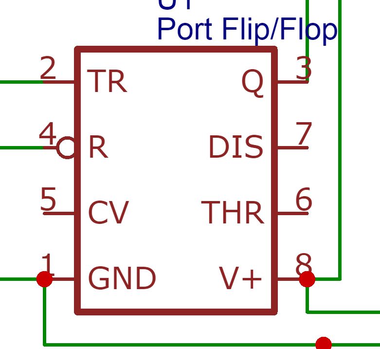
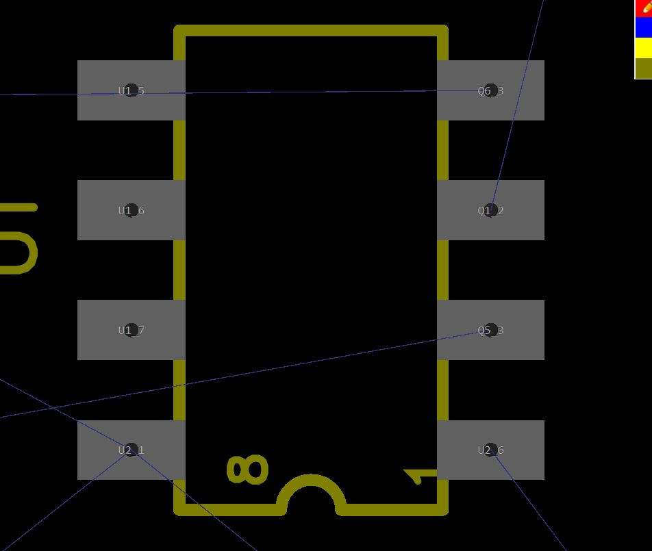
When I build my board in the schematic I wired it accordingly to the correlating pins, however when converted to PCB the pins are not only flipped, but they don't share the same orientation. Meaning, it's not a mirror image, they completely change location! Which cannot be fixed with just a re-wire on the PCB because the chip itself won't match. Am I missing something? ![Schematic.jpg](//image.easyeda.com/pullimage/UerDJv6HbK2es2FJ2p9LUBVCaxr5hQyiDI3eNbqF.jpeg) ![PCB.jpg](//image.easyeda.com/pullimage/SMOcBG1yn0lpQwCyz4db2sHLkLs8otsdMiJrRgNz.jpeg) Thank you for any help....as I said, I'm new, keep that in mind if responding with help! Kind regards, Ryan
Comments
andyfierman 5 years ago
There's not enough info in your screenshots and description to make out what's happening. The schematic does not show other devices that the pins are connected to. The PCB has auto-assigned netnames that are based on the pins from which the wire connections in the schematic start. The footprint in the screenshot gives no indication of the pin numbers to check that the schematic symbol and PCB footprint pin assignment is correct. * Can you post the link to this as a public project? In the meanwhile, please see: [https://easyeda\.com/andyfierman/Welcome\_to\_EasyEDA\-31e1288f882e49e582699b8eb7fe9b1f](https://easyeda.com/andyfierman/Welcome_to_EasyEDA-31e1288f882e49e582699b8eb7fe9b1f)
Reply
andyfierman 5 years ago
You can check the connectivity using the Design button to access the Schematic and PCB Design Managers. You can also Cross Probe between the Schematic and the PCB using the Cross Probe Tool (Shift+X).
Reply
ryan1776 5 years ago
* Can you post the link to this as a public project? Actually, I'm designing this as a project that I hope to make a little side cash on. So I don't want to post it in it's entirety. I was hoping just showing that the pins were swapped would be enough to tell me, "yeah it's a glitch" or "that's what it's supposed to do" or You're an idiot and doing it wrong! lol You can see just by the numbers that 8 and 1 are reversed. Schematic-Down the left side only one pin is left open CV (control voltage) and on the right discharge and threshold. But on the PCB you can tell there's three pins on the left that are not wired. And all on the right are wired. Regardless of what the traces are going to, that's incorrect as the 555 chip won't be oriented that way. Ah well, thought I'd try.
Reply
andyfierman 5 years ago
@ryan1776, You have to understand that a PCB is not a 1:1 mapping of the schematic or vice versa. For more on this please see (2.2) in: [https://easyeda\.com/andyfierman/Welcome\_to\_EasyEDA\-31e1288f882e49e582699b8eb7fe9b1f](https://easyeda.com/andyfierman/Welcome_to_EasyEDA-31e1288f882e49e582699b8eb7fe9b1f) Suppose we take the schematic symbol for the 555\_BJT\_EE Schematic symbol: ![image.png](//image.easyeda.com/pullimage/tV1H3K42hbetpVO342ei1dGZSgRnmWV5eRzU1jBv.png) Note that although the pin numbers are the same as those of the physical package, the pin positions are arranged to make for a clear, easy to use and to read symbol and are not necessarily in the same order as those on the physical package. Suppose you want to use the SOIC-8(6.27X3.91) PCB footprint to this symbol: ![image.png](//image.easyeda.com/pullimage/gAoykSDIzK80CMGbOKKYGrx2yCIHwcHfcwPBSrKY.png) Note how the pads are numbered sequentially, anticlockwise around the PCB footprint the same way they are on the physical package. So, place and then select the symbol in the schematic and click on the package attribute... ![image.png](//image.easyeda.com/pullimage/TocLPz8Vxuu6zS45MPwixYUlLydHUCHoGY0D1eJT.png) To open the Footprint Manager in which you can assign the footprint to it. The Footprint Manager which will then show how the symbol pins map to the footprint pads: ![image.png](//image.easyeda.com/pullimage/7l6I8gSPP6jQ9c0VqZ8qNp3RbNT6Yt9JewrejIH9.png) Note that the symbol and footprint mapping is numerically correct. If you look at your screenshots you'll see that the unconnected pins on the footprint correspond to the unconnected pins on the symbol. From your screenshots, it is not possible to check where the connected pins go but if you have constructed the schematic correctly then when you convert it to a PCB, they **will connect** to the same pins in the PCB as you have drawn them to in the schematic. Obviously that does not guarantee that the connections are right to make your circuit actually work but that is down to how accurately you have drawn the schematic rather than the tool itself.
Reply
ryan1776 5 years ago
Thank you for that very detail answer! Helped tremulously. Why is it like this though? Why wouldn't the schematic match the packaging of the chip? Then when things are being designed it will match the actual chip? Seems like extra work the way it's currently done.
Reply
andyfierman 5 years ago
If you read section 2 in the Welcome to EasyEDA project you'll see why. The rules that make a schematic easy to construct and read are very different from the rules that govern successful PCB layout.
Reply
Login or Register to add a comment
goToTop
你现在访问的是EasyEDA海外版,使用建立访问速度更快的国内版 https://lceda.cn(需要重新注册)
如果需要转移工程请在个人中心 - 工程 - 工程高级设置 - 下载工程,下载后在https://lceda.cn/editor 打开保存即可。
有问题联系QQ 3001956291 不再提醒
svg-battery svg-battery-wifi svg-books svg-more svg-paste svg-pencil svg-plant svg-ruler svg-share svg-user svg-logo-cn svg-double-arrow -mockplus- -mockplus- -mockplus- -mockplus- -mockplus- -mockplus- -mockplus- -mockplus-@1x -mockplus-

Cookie Notice

Our website uses essential cookies to help us ensure that it is working as expected, and uses optional analytics cookies to offer you a better browsing experience. To find out more, read our Cookie Notice