@andyfierman
Thank you for your interest in replying.
This is my first experience with EasyEDA. I have several mechanical components to place on a two-sided 3-1/2" diameter PCB and need to position ICs appropriately to avoid them. I have very detailed pad locations and mechanical component pin locations from data sheets for each of my components appropriately positioned on my PCB as generated in my drafting program (MadDraft), ready to export to EasyEDA as a single image in DXF format. With coaching I could either superimpose my EasyEDA schematic or draw my own traces to complete the PCB design and generate Gerber files.
To get the best out of EasyEDA and to help preserve everyone sanity, the first thing to do is to read (2) (Welcome to EasyEDA) in:
[https://easyeda.com/forum/topic/How-to-ask-for-help-and-get-an-answer-71b17a40d15442349eaecbfae083e46a](https://easyeda.com/forum/topic/How-to-ask-for-help-and-get-an-answer-71b17a40d15442349eaecbfae083e46a)
Then study (2.2) and (2.3) in (2) (Welcome to EasyEDA) in that document.
Then follow the Design Flow in (1) (the Tutorial) in (2) (Welcome to EasyEDA) in that document.
Having done that, start by searching for and if necessary, building the PCB Footprints and the Schematic Symbols that you need for your project.
Then create a Schematic.
Go through the checklist (4) before converting to PCB.
Then do Convert to PCB...
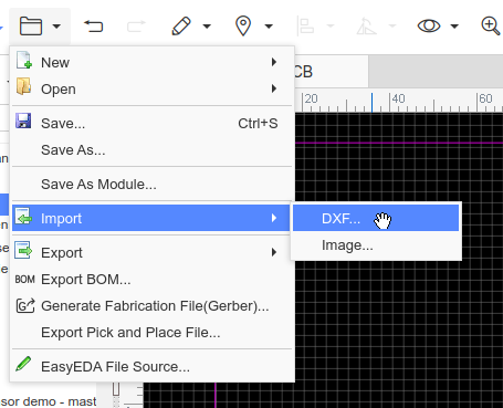
Then, you should be able to import the DXF into the Document or Mechanical layers of the PCB.
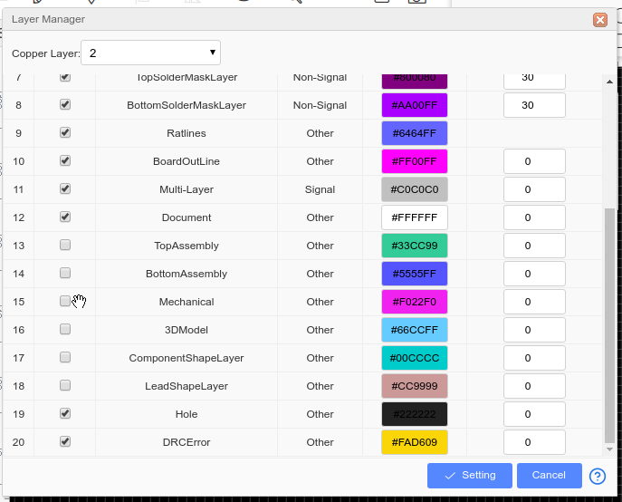
How to show the Mechanical layer in the Layers pallete:
Then modify or delete the default Board Outline to create the circular one you want.
Then using the DXF as a template, position the parts that have been pulled into the PCB from the library.
Don't forget: if it is on or forms an integral part of the PCB then there must be the PCB Footprint for it and a Schematic Symbol for it with that footprint assigned to it which must be in the Schematic. Then when you do Convert to PCB... everything is pulled into the PCB and all you have to do is push it about to the required position and then just route the copper tracks.
Then go through the checklist (6) in (2) (Welcome to EasyEDA) before you order the PCB.
Doing a project in any other way will be unnecessarily painful and if you then ask for help is just unfairly wasting everyone's time.
Have fun!
:)
Our website uses essential cookies to help us ensure that it is working as expected, and uses optional analytics cookies to offer you a better browsing experience. To find out more, read our Cookie Notice


 Brand new interactions and interfaces.


 Easy to use and quick to get started.