At times I need pads to be removed from stencil and solder mask and there is no solution right now except editing gerber files. Please add new properties to pads Disable/No Solder Mask, Disable/No Paste Mask. Thanks.
You can not? Every pad has paste mask, I can only expand it in pad properties, but not remove. Am I missing something and you can remove mask from a pad in EasyEDA?
Yes, you can only edit the expansion, you can't delete it. you can use solid region instead of this pad.
multi-layer pad doesn't have the paste mask, or you can change this pad to multi-layer
To clarify,
The EasyEDA PCB Editor allows:
1. automatically placed Solder and Paste Mask apertures to be expanded but not deleted;
2. Additional Solder and Paste Mask apertures to be created and edited.
Note that:
(a) additional Solder Mask apertures can be created independently in any shape including as text and in any location;
(b) additional Paste Mask apertures can be created independently in any shape (except as text) and in any location even if they are non-sensical.
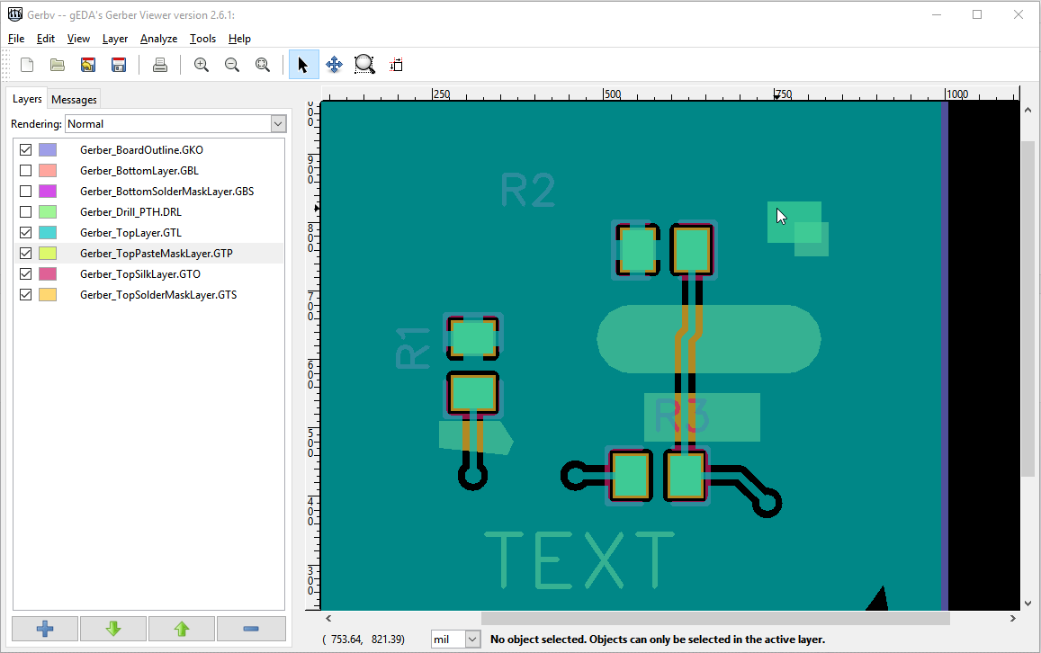
The screenshots below show the EasyEDA PCB view and the Gerbers of a test PCB with several additional Solder Mask apertures (including one as text) and in the upper right corner, a small rectangler aperture of Solder Paste Mask overlapping a small rectangular aperture of Solder Mask. This means that it is possible (but non-sensical!) to place an aperture in the Solder Paste Mask layer over an area that is covered by Solder Mask (i.e. not over exposed copper).
EasyEDA PCB Editor view:

Gerbers in gerbv:
@UserSupport I'd love to use solid regions, except you can't number them in PCB libraries, so it's physically impossible to create a paste-mask-less footprint.
Our website uses essential cookies to help us ensure that it is working as expected, and uses optional analytics cookies to offer you a better browsing experience. To find out more, read our Cookie Notice


 Brand new interactions and interfaces.


 Easy to use and quick to get started.