You need to use EasyEDA editor to create some projects before publishing
Autorouter won't make connections to switch
382 9
Andrew Melbourne 2 years ago
Hello! I have just begun an internship and have been tasked with updating an old PCB. I replaced over 80% of the original parts and nearly all the original tracks were unrouted. I have everything placed to our satisfaction and everything autoroutes okay except for 6-8 traces all connected to a switch with a custom footprint that I canno't replace. I believe it is this footprint that the autorouter is having trouble with. Any advice on how I could modify this to work would be greatly appreciated! Note: Manual routing the tracks after the autoroute completes is my last last resort, whenever I have tried it ends up being very messy. Really would like to avoid this. ![Screen Shot 2021-05-17 at 11.01.54 AM.png](//image.easyeda.com/pullimage/MyePrDf36jYu6Nt6BsKyDtmR6PXrfifb5Ba2ExOp.png) 
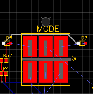
Clearly routable connections aren't made. I must assume its the footprint ![IMG_6002.jpg](//image.easyeda.com/pullimage/VPShtfOVCCgYR0V5nN0xa2ZbE9h4fDCikaEdV03O.jpeg) 
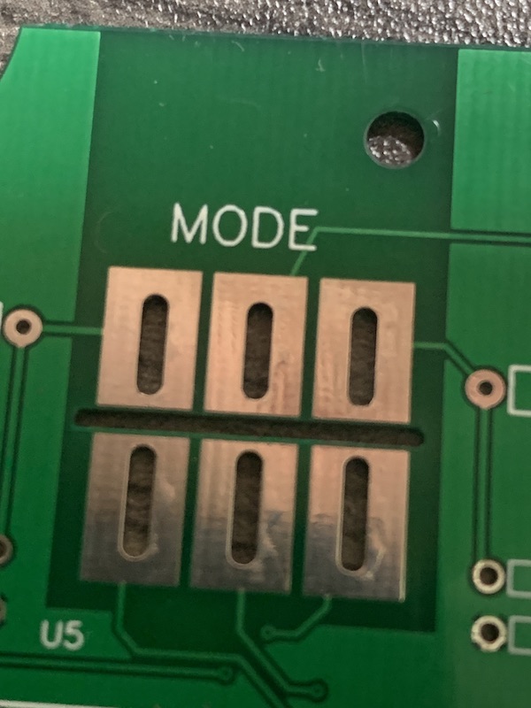
Footprint on an old version of the board. Plating on top layer only Thanks so much!
Comments
andyfierman 2 years ago
It is not clear from your post if this is a PCB that was originally designed in EasyEDA and which you are updating or if it is a design that you have recreated from scratch in EasyEDA. Since all footprints and schematic symbols are public in EasyEDA, please identify it clearly in the Library and post a screenshot that includes the whole Library window. Please do the same for the schematic symbol associated with it in the schematic. The quickest way to solve this is to see your project. If you can, please make the project public and post the url to it back here. If not you could add me (andyfierman@easyeda.com) as an observer to your project.
Reply
Andrew Melbourne 2 years ago
@andyfierman Thank you for your reply! The PCB was originally designed in EasyEDA. Footprint: ![Screen Shot 2021-05-17 at 2.09.27 PM.png](//image.easyeda.com/pullimage/x1P0XD59vQN8k8grOh47uJOtDVevhazJVOGgmbGI.png) Symbol in schematic: ![Screen Shot 2021-05-17 at 2.05.53 PM.png](//image.easyeda.com/pullimage/d4el6EghQ4Hd5wMkdoHowbQq6MsAVjEDonH4prfb.png) Unfortunatley, I am unable to share anything beyond these screenshots. Thank you so much for the consideration.
Reply
andyfierman 2 years ago
Can you identify the switch symbol in the library?
Reply
andyfierman 2 years ago
Another thought. Can you make a dummy project that just includes tge switch and the nets around it and a PCB made from it that demonstrates the issue? Then share that?
Reply
Andrew Melbourne 2 years ago
@andyfierman Great idea. I have shared that with you. Thanks a ton.
Reply
andyfierman 2 years ago
@melbourneandrew, Can you post the url to it?
Reply
Andrew Melbourne 2 years ago
@andyfierman [https://easyeda.com/editor#id=574ae54f16654611acf126822a3d8036](https://easyeda.com/editor#id=574ae54f16654611acf126822a3d8036)
Reply
andyfierman 2 years ago
Ah! Got it: you added me to the project. I can see that now. :)
Reply
andyfierman 2 years ago
Based on your example, the short answer is that the footprint has been created to be placed ion the top layer but has pads only on the bottom layer so your top layer surface mounted components cannot connect to them without adding vias to swap layers. However, I don't understand how in your original design the pads appear to be on the top layer along with D3, D6, R4 and R57. The longer answer is that the footprint is not well constructed. It does not conform to the requirements in this How To: [https://easyeda.com/forum/topic/How-to-avoid-DRC-errors-when-connecting-to-PCB-Footprints-a-k-a-PCB-Libs-90bf944fe3644b21a7d27a9e9d8df8d6](https://easyeda.com/forum/topic/How-to-avoid-DRC-errors-when-connecting-to-PCB-Footprints-a-k-a-PCB-Libs-90bf944fe3644b21a7d27a9e9d8df8d6)<br> <br> The quickest way to fix this, is to edit the footprint to add a second small, single layer pad to each of the 6 pads. They can be round or rectangular but small enough to place at the outer end of each of but inside the boundary of the exisiting recyangular pads. The new pad must have the same number as the pad it is surrounded by. To avoid it snapping straight ot the original pad centre place the new pad outside in the Footprint Editor canvas then reselect it and drag it where you want. Then when you do right-click Update on the footprint in the PCB it should pull in the edited version and the tracks should be able to route to the new secondary pads. Another, tidier but more complex solution is to rebuild the existing pads as polygons but manipulate the points so that the effective pad centre is offset to one end to move the snap point out of the Solid Region set to Cutout. If you can accept having pads on both sides of the board with plated through holes (which is actually the correct way to make footprints for through-board pins), then rebuild the pads as slotted rectangular or oval multilayer pads and delete the Solid Regions used to form the slots in the pads (keep the one for the centre line slot). Try to get the datasheet for the switch so that you can check the footprint dimensions anyway. Then for your own sanity, do the essential checks in (4) and (6) in (2) in: [https://easyeda.com/forum/topic/How-to-ask-for-help-and-get-an-answer-71b17a40d15442349eaecbfae083e46a](https://easyeda.com/forum/topic/How-to-ask-for-help-and-get-an-answer-71b17a40d15442349eaecbfae083e46a) Ideally read all of it and the linked documents but you may not have time to get through all of it. :) Questions? Just ask.
Reply
Login or Register to add a comment
goToTop
你现在访问的是EasyEDA海外版,建议访问速度更快的国内版 https://lceda.cn(需要重新注册)
如果需要转移工程请在个人中心 - 工程 - 工程高级设置 - 下载工程,下载后在https://lceda.cn/editor 打开保存即可。
有问题联系QQ 3001956291 不再提醒
svg-battery svg-battery-wifi svg-books svg-more svg-paste svg-pencil svg-plant svg-ruler svg-share svg-user svg-logo-cn svg-double-arrow -mockplus- -mockplus- -mockplus- -mockplus- -mockplus- -mockplus- -mockplus- -mockplus-@1x -mockplus-

Cookie Notice

Our website uses essential cookies to help us ensure that it is working as expected, and uses optional analytics cookies to offer you a better browsing experience. To find out more, read our Cookie Notice