You need to use EasyEDA editor to create some projects before publishing
C390032 - Polarity reversed
629 16
EdHayes3 2 years ago
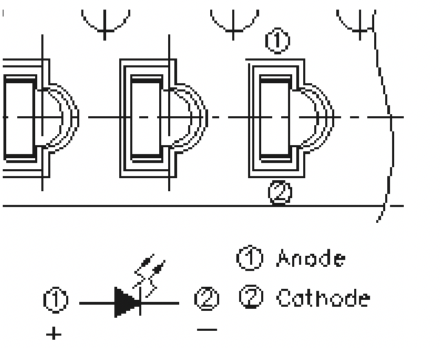
I sent a message to support about this, and they are saying this is correct. But it is clearly not. The polarity expressed in the data sheet does not match the EasyEDA symbol/footprint Datasheet ![image.png](//image.easyeda.com/pullimage/Gl1GE0ZRwLOKr9UDFpDksSz9WrlgbKenxdsrV2Ke.png) EaseyEDA ![image.png](//image.easyeda.com/pullimage/iZtmoH6fgQWfRLiMECvd1gFcgfejuvCkjI9VBX6v.png) ![image.png](//image.easyeda.com/pullimage/mMyNQn3SRwLShSEz3w2bBXK5d5tWrKI3eyWPwYR5.png)
Comments
andyfierman 2 years ago
@EdHayes3, Please post the link to the device datasheet.
Reply
andyfierman 2 years ago
@EdHayes3, Sorry but I do not understand the problem. The polarity of symbol and the footprint for the LKIR30102C-A02(DY), LCSC Part # C390032, are correct to the datasheet: [https://datasheet\.lcsc\.com/lcsc/2010221806\_Everlight\-Elec\-LKIR30102C\-A02\-DY\_C390032\.pdf](https://datasheet.lcsc.com/lcsc/2010221806_Everlight-Elec-LKIR30102C-A02-DY_C390032.pdf)<br> <br> from: [https://lcsc\.com/product\-detail/Infrared\-IR\-LEDs\_Everlight\-Elec\-LKIR30102C\-A02\-DY\_C390032\.html](https://lcsc.com/product-detail/Infrared-IR-LEDs_Everlight-Elec-LKIR30102C-A02-DY_C390032.html)<br> <br> ![image.png](//image.easyeda.com/pullimage/RIHy1qeQs03tSnHw00a7vn4vjiomKyiDzpfLJX81.png) There is however a slight issue that the footprint has three pads whereas the symbol only has two so there may be a DRC error for the unconnected pad on the PCB. :)
Reply
EdHayes3 2 years ago
Hi Andy. Look at the bottom of the datasheet where it shows the reel details. Page 8. Part of my conversation already sent to LCSC support was that the top and the bottom of the datashet do not match. I also sent a note to Everlight. I've been told it's all correct. But You certainly have found, likeyly, why the footprint polarity is the way it is.
Reply
deskpro256 2 years ago
Hi, I'm really trying, but I can't see a problem here at all. The polarity is correct, the symbol and footprint is also ok. In the reel it is also noted in which orientation they are coming, seems alright to me. Here you can see that there are 3 pins to the symbol in EasyEDA: ![Screenshot_1.png](//image.easyeda.com/pullimage/D2VinrnITR4riIFqgmoF2i5vgb5JTmFvnYVBR9tc.png) ![Screenshot_2.png](//image.easyeda.com/pullimage/ltrSIc1GxAU2NFlczSeQrIRKOlTNxD7jxX3FRKqB.png) ![Screenshot_3.png](//image.easyeda.com/pullimage/ARtNeGXB7wcdZLVrjlbuIfv6c8CuOwssf93OC4Tx.png) And don't mistake that triangle as the diode "triangle", it is a marker, not a directional arrow which points from anode to the cathode. Unless there is something I'm missing, you might be in too deep and need to sleep :D
Reply
andyfierman 2 years ago
@EdHayes3, This picture in the datasheet shows the schematic symbol pin to physical device package pad mapping: ![image.png](https://image.easyeda.com/pullimage/RIHy1qeQs03tSnHw00a7vn4vjiomKyiDzpfLJX81.png) The picture below, from near the end of the datasheet is not intended to be used to indicate the relationship of the symbol pin to package pads. It only shows the orientation in which the physical device is loaded into the tape when reeled and the direction of feed into a pick and place machine: ![image.png](//image.easyeda.com/pullimage/pNE9FsWUtYPyhP4ey8M1ROEnqy9r8w951PaIA04r.png) This information is necessary in order to correctly orient the device onto a PCB. The physical orientation of the packaged device is independent between the two pictures and, since the two "sides" are not distinguished in either picture, there is no contradiction between the side views presented in the two pictures: simply flipping the device between the two pictures will produce the apparent change of pin order that seems to be confusing you but will of course have not effect on the pin to pad mapping. I put "sides" in quotes because it is unclear from the description and the images whether this device is: 1. vertically mounted (it is described as a LED "with spherical top view lens" in which case the flat faces form the "sides" of the package with the pads on the bottom face) or; 2. side mounted (it is shown in the recommended pad drawing as being side mounted in which case the flat faces form the interchangeable Top and Bottom of the package).
Reply
EdHayes3 2 years ago
If the part was simply taken out of the packag with a pick and place machine, and placed on a PCB, the footprint this part is using in EasyEDA would not work. And I believe 99% of the use of this part would follow that process. Using the birds eye view, where the light emmiting lense is on the top, the negetive/cathod is on the right, not left. That's the problem. I've never seen a PNP machine that would rotate a part 90 degrees on the Z axis (or 180 degrees for that mater). I'm not sure why anyone would place this part on a board with the rounded section facing up. It's quite possible the datasheet was put together sloppily, where parts were reused from previous datasheets and was not properly validated. I'm not sure. The datasheet may not be wrong, to the literal sense of the word, as you said nowwhere does it say the depeiction is a birds eye view of the part, but the top section is uninutitive/deceiving. The bottom section does show which side is which. ![image.png](//image.easyeda.com/pullimage/UpWLZ1ipIzlKcYAdbf3gcToGjP8iSeRNcFO8qzeF.png) Doesnt match: ![Screenshot_3.png](https://image.easyeda.com/pullimage/ARtNeGXB7wcdZLVrjlbuIfv6c8CuOwssf93OC4Tx.png) I guess the question is: If I use the EasyEDA library item for this part, and order JLCPCB board production with P&P, and its wrong, what happens? They have confirmed everything is correct. But when I bought LCSC parts, and put on my JLCPCB board, I had to flip each LED. Not terrible for one or two prototypes, but for larger run of assembled prototypes, that could be a problem.
Reply
EdHayes3 2 years ago
FYI, picture of product. ![2017_0620_065604_001.JPG](//image.easyeda.com/pullimage/tbuspyR1N6QWyUm9ccfwJEpMckA4S6PfqpaQtU7A.jpeg)
Reply
deskpro256 2 years ago
Oh yeah, I see it now. The footprint is wrong for PnP use. @UserSupport Could you take a look at this again? The fix is simple, switch the pins in the footprint, so it lines up. Until that is fixed, your best choice could be switching the pins manually in your PCB or cloning that part and fixing it yourself, then using the LCSC part in the PnP file.
Reply
andyfierman 2 years ago
@EdHayes3, @UserSupport, Yes I get it too now. It needs the Footprint to be corrected. * The Everlight datasheet could do with being clarified too, to make it clear in the description that the device is a side mounted LED. Maybe somebody at LCSC or JLCPCB could contact Everlight do that.
Reply
EdHayes3 2 years ago
FYI, sister part C390033 has the exact same problem. If I were to find simialr issue with other parts, what's the best way to report this? I'd hate to go through a similar process for each one.
Reply
andyfierman 2 years ago
@EdHayes3, Use the Report Error tool: ![image.png](//image.easyeda.com/pullimage/WGt7atNVyd4v2aPiitw6xWJaYqHF8bAJrD83lUe8.png) or: ![image.png](//image.easyeda.com/pullimage/eNx1M4pMpaTp0WykxEZDEAGPFmZnUGKu8dJlQze5.png)
Reply
andyfierman 2 years ago
@EdHayes3, I was talking rubbish about the symbol not having 3 pins to map onto the three pads of the device: it does. Sorry about that.
Reply
andyfierman 2 years ago
@EdHayes3, Can you post some more photos of the LEDs out of their reel tape, showing both of their their sides? @UserSupport, Isn't there another problem with this part? If you look closely at the datasheet: ![image.png](https://image.easyeda.com/pullimage/RIHy1qeQs03tSnHw00a7vn4vjiomKyiDzpfLJX81.png) and at Ed Hayes photo of the part: ![2017_0620_065604_001.JPG](https://image.easyeda.com/pullimage/tbuspyR1N6QWyUm9ccfwJEpMckA4S6PfqpaQtU7A.jpeg) the pads on the device do not look like they wrap round onto the side of the package. The pads appear to be only on the "bottom" of the package, i.e. the side of the package opposite the lens face. If that is true then how is this device soldered at right angles onto a set of pads so that it is side facing?
Reply
EdHayes3 2 years ago
@andyfierman, no worries. about the pad qty. The part looks the same from the top and bottom. There's no horizontal metal surface. I think it's held in place by the solder fillet.
Reply
andyfierman 2 years ago
"I think it's held in place by the solder fillet." It might be possible to assemble it that way but no way would that ever pass any sort of QA let alone IPC standards.
Reply
UserSupport 2 years ago
@andyfierman @EdHayes3 Got it, we will check and fix it ASAP Thank you
Reply
Login or Register to add a comment
goToTop
你现在访问的是EasyEDA海外版,使用建立访问速度更快的国内版 https://lceda.cn(需要重新注册)
如果需要转移工程请在个人中心 - 工程 - 工程高级设置 - 下载工程,下载后在https://lceda.cn/editor 打开保存即可。
有问题联系QQ 3001956291 不再提醒
svg-battery svg-battery-wifi svg-books svg-more svg-paste svg-pencil svg-plant svg-ruler svg-share svg-user svg-logo-cn svg-double-arrow -mockplus- -mockplus- -mockplus- -mockplus- -mockplus- -mockplus- -mockplus- -mockplus-@1x -mockplus-

Cookie Notice

Our website uses essential cookies to help us ensure that it is working as expected, and uses optional analytics cookies to offer you a better browsing experience. To find out more, read our Cookie Notice