Yes and no.
See:
IMAGE\_AS\_PAD\_DO\_NOT\_USE
in the user contributed PCB Libs.
You cannot import an image directly as a pad.
You can import it into the top or bottom layer and then place a pad into it but on placing the completed PCB Footprint into a PCB, it will generate DRC errors where tracks enter and leave the copper are defined by the image.
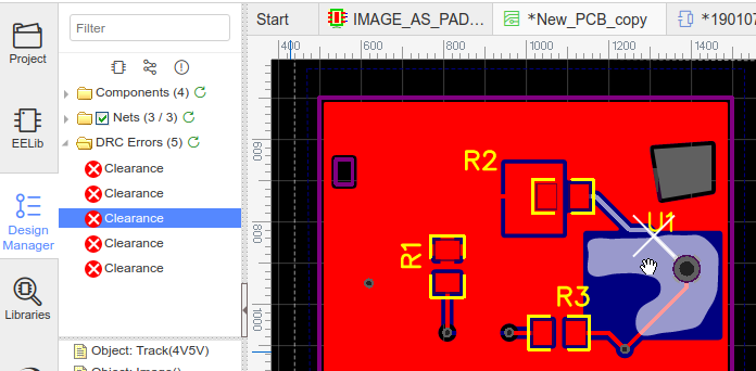
* This is because it is not possible to assign a pad number to anything that is not a pad and anything that does not have a pad number will generate a DRC error when placed into a PCB.
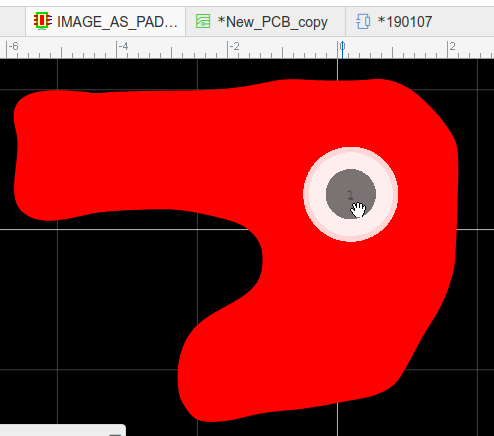
Thanks. The idea was based on turning my business logo into a pad as i think it would be aesthetically pleasing when it gets the silver of the tin on it. What you have mentioned here would not work for that would it as the solder mask needs to be kept off it also...
Ah. That's easy!
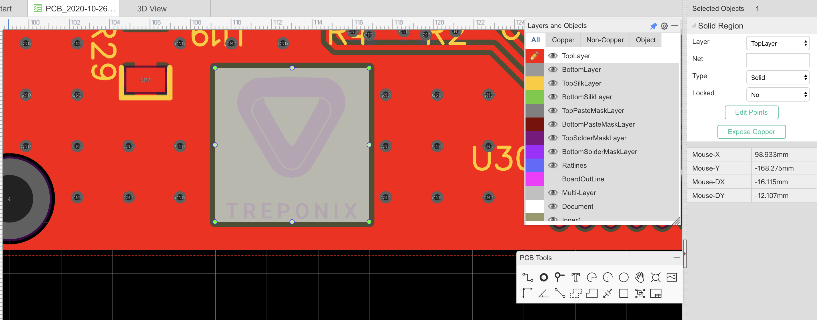
Import it as a **Solid Region** set to **Solid** then click on the **Expose Copper** button in the right hand panel.
Try it and check the Gerbers using gerbv.
:)
You're quite right.
My bad.
Still easy but it's a slightly different way to achieve what you want.
Suppose you want this on the Top layer.
1. Import the image into the copper layer;
2. Copy it the copper into the Top SolderMask Layer;
3. Position both to the same desired location using the XY co-ordinates.
You have copper and you have a solder mask aperture placed directly over it.
JLCPCB will put whatever finish that you select when you submit the order for the PCB.
Please ensure that you follow the checklists in (4) and (6) in (2) in:
[https://easyeda.com/forum/topic/How-to-ask-for-help-and-get-an-answer-71b17a40d15442349eaecbfae083e46a](https://easyeda.com/forum/topic/How-to-ask-for-help-and-get-an-answer-71b17a40d15442349eaecbfae083e46a)
and in particular check using gerbv, that the Gerbers show the expected aperture in the relevant soldermask over your logo.
* Note that you should probably create this copper area and soldermask aperture as a PCB Footprint and then also create a Schematic Symbol with the name of that PCB Footprint assigned to it. Place the symbol on your schematic and then do **Import Changes...** or **Update PCB...** to pull the logo footprint into the PCB.
If you just put the logo directly into the PCB, it may be deleted if you do **Import Changes...** or **Update PCB...**.
This is explained in more detail in references (2.2 and 2.3) in (2) in the above post.
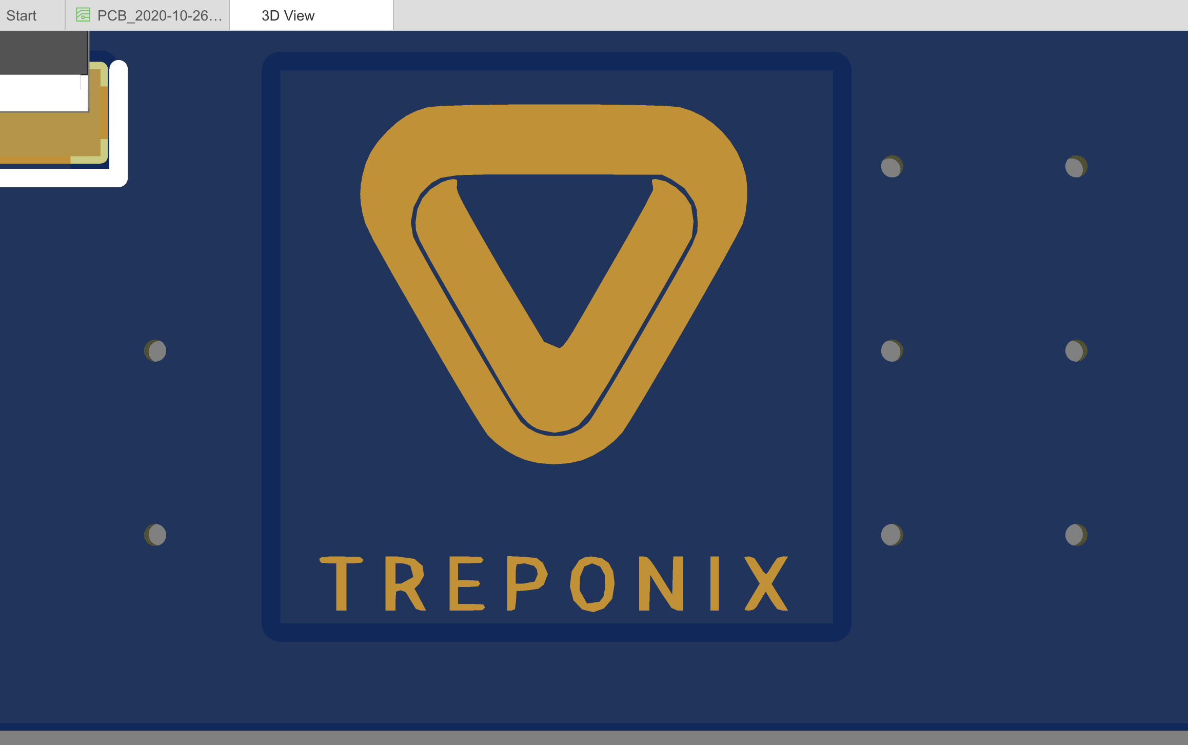
@andyfierman: Is it also possible to create a solid region on the Toplayer, connected to no net and adding then the logo on the region on the TopSolderMaskLayer?
In the PCB preview it is not visible but in the 3D preview it is. We would like to have the logo placed on the PCB like in the 3D preview but we are not sure if our method of logo placing is correct.
@ManuelPossegger
That should work fine.
Install a copy of gerbv as advised in the Tutorial and then check your Gerbers using that.
Here's where to get gerbv for OS X from:
[http://www.ghz.cc/charles/fink/#gerbv](http://www.ghz.cc/charles/fink/#gerbv)
BTW: Nice logo!
@ManuelPossegger,
Obviously, other gerber viewers are available but I know gerbv works properly.
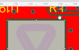
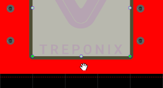
I note that you have extensively stitched you plane area. If this is important for your design then rather than disrupt the continuity of the ground(?) plane with the isolated solid region, you might prefer to just have a border round the logo then you also have more freedom in where you can place it.
In your image above, the solid region has restricted the plane area as indicated below:
:)
@andyfierman We got your concerns but in our design the logo is placed in the very left down corner and the main ground plane above the logo is still big enough. We just wanted to seperate the logo from the ground plane so that nobody has access to the schematic through any exposed copper areas. So we just wanted to separate any areas with important potential from logo stuff - even if it is only GND. Regarding the stitching in that area: it is only a little important for small current of an IC and not that important for EMI.
:)
Our website uses essential cookies to help us ensure that it is working as expected, and uses optional analytics cookies to offer you a better browsing experience. To find out more, read our Cookie Notice


 Brand new interactions and interfaces.


 Easy to use and quick to get started.