The title pretty much says it all, i am doing a VCF project and everytime i connect the pins, Easyeda just deletes them.
I really can't seem to find a solution to this problem, and it is giving me a headache, so now i went to ask here.
Please give more information.
Are you talking about a schematic or a PCB?
If schematic then which LM13700 symbol are you using?
Which PCB footprint is assigned to the symbol?
If PCB then which PCB footprint are you using?
Can you make your project public?
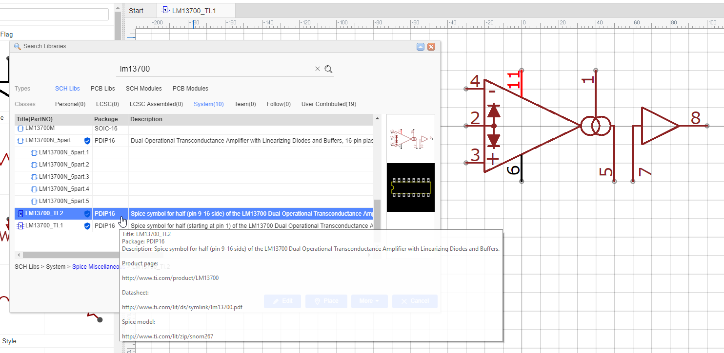
It is in a shcematic, and i am using the standard LM13700 symbol (im pretty sure it is the first that comes up when you search it in the libarary), however i also tried the LM13700_TI one and two. The footprint is the PDIP16. I also made the project public now.
I am pretty new to Easyeda.
Sorry for the inconvinience.
OK, understand the issue now.
The problem seems to be that because pins 5 and 7, and pins 12 and 10 are effectively internal to the symbol, it's not possible to wired directly between them.
The symbol was created to try to simplify the representation of the two sections of each half of the LM13700 but it was not apparent that this problem could arise.
There is however, a simple workaround which actually makes for a more readable schematic anyway.
:)
Move the C3 down a couple of grid points then wire from pin 5 to the top of the cap:

Then wire from pin 7 to the wire corner:

and the wires stay put:

Then do the same for pin 12 to C5 and pin 10.
@UserSupport,
That might be the simplest way to do it.
Making it a 5 sub-part symbol so that the two amplifiers stages, the two output buffer stages and the power supply pins are on separate symbols would be even nicer.
Then the two amplifier sub part symbols will have only the two differential input, the control input, the output pins. The two buffer sub part symbols will just have an input and an output pins and a 5th power supply pins sub part symbol will just have the positive and negative supply pins.
Just updated LM13700\_TI\.1 and LM13700\_TI\.2 symbols to make the pin 5 \- 7 and 10 \- 12 pin wiring work on these simulatable symbols\.
Our website uses essential cookies to help us ensure that it is working as expected, and uses optional analytics cookies to offer you a better browsing experience. To find out more, read our Cookie Notice


 Brand new interactions and interfaces.


 Easy to use and quick to get started.