I'm not sure when this feature was introduced but a first attempt at PCB component autoplacement now operates after doing a multiple component selection in the schematic followed by a CTRL+SHIFT+X Cross-Probe-and-Place.
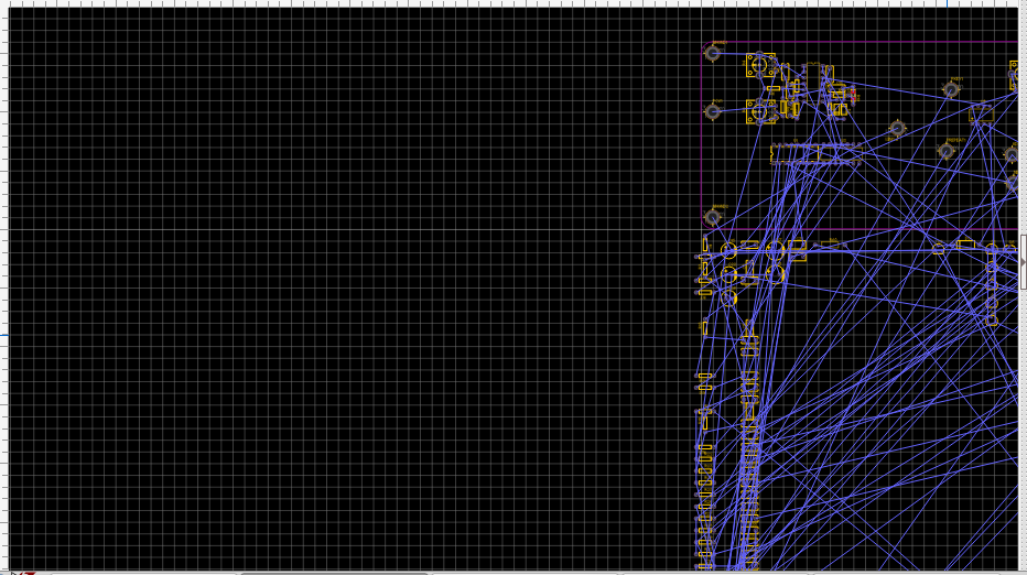
This is the board shortly after the initial Create PCB:

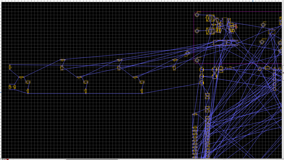
I then selected a collection of components in the schematic (sorry but it's private so I'm not going to show that) and did CTRL+SHIFT+X Cross-Probe-and-Place and this is how the components were distributed:

which is pretty much exactly as they are laid out in the schematic.
Now, that may not be much like they will end up being placed as it's around two quad-device packages in the upper right that all the ratlines go to but it's a far easier task to lay them out from this arrangement that from the alphanumerical prefix ordered columns that they get pulled into the PCB in the first place.
* To do a whole board do CTRL+A (Select All) then do CTRL+SHIFT+X.
* Your PCB must have been saved before this will work.
Well done EasyEDA, this is a big step forward to help speed up PCB layout.
Big thank you!
Chrome
81.0.4044.138
Ubuntu
EasyEDA
6.4.0


