You need to use EasyEDA editor to create some projects before publishing
Components with a ground net not connecting to ground plane?
1170 4
GeoffGrauer 1 year ago
Hello everyone, having this weird issue and can't seem to figure out how to solve it. 
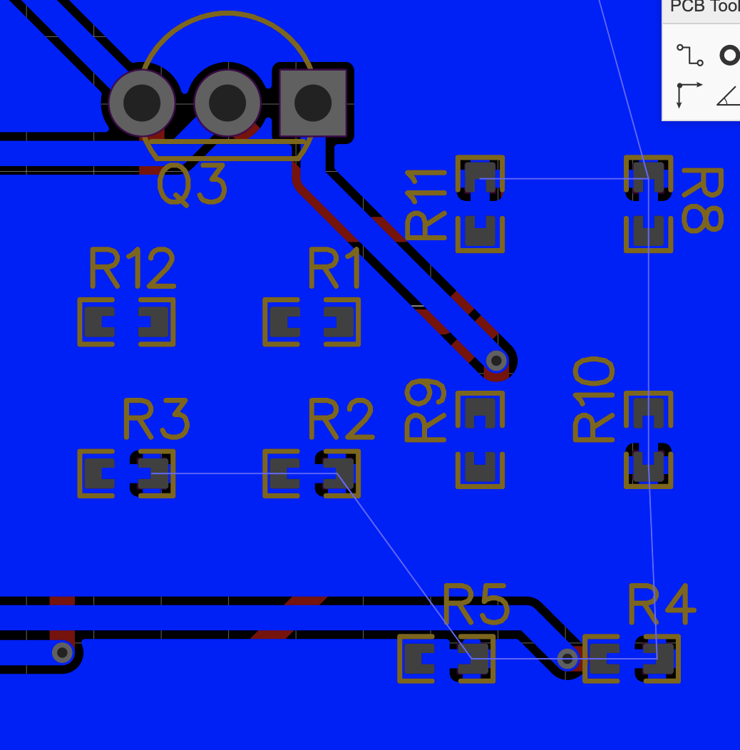
I have a number of components that are connected at one end to ground. I have that on the schematic, when I'm in the PCB editor and click on that pad the sidebar tells me its connected to ground, and they're all labelled as GND when you zoom in. However after I have everything routed and created a ground plane I still have the thin lines connecting the ground pads of these components as if they're not properly connected. I don't want to order PCBs only to not have them pbe properly connected like I want them to be. I've done a couple other schematics and not had this problem before. Any suggestions? Thanks!![Screen Shot 2022-06-08 at 4.41.38 PM.png](//image.easyeda.com/pullimage/H80pYX27IaeqlaOJO0g69Hq89b4yuKg1lrHVa5yq.png) 
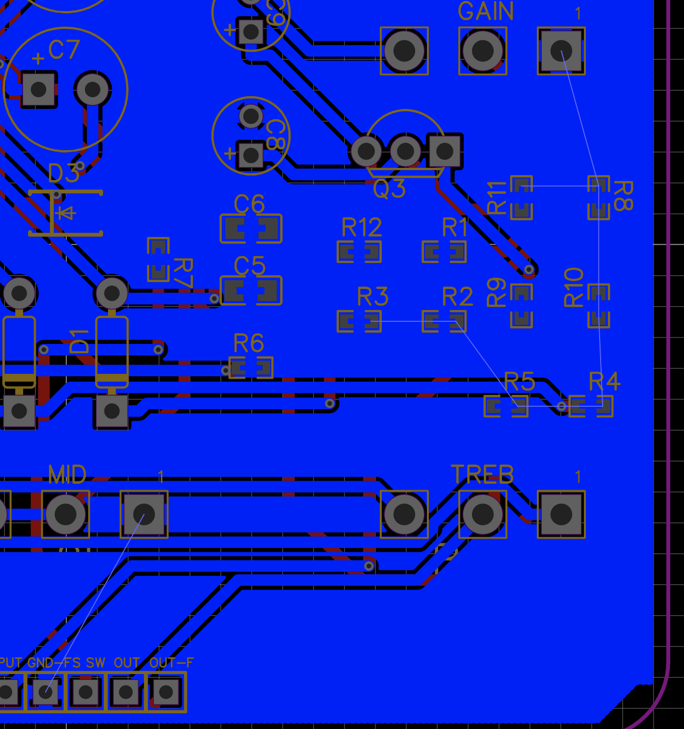
EDIT: So I'm not sure what I did but now the resistors are showing as being connected to the ground plane. However the lines are still there and the DRC still says that its an incomplete circuit. ![Screen Shot 2022-06-08 at 6.25.47 PM.png](//image.easyeda.com/pullimage/5juEOp8oBLtW1E9DAPlUv16AgBSFhcY4r785LosE.png)
Comments
andyfierman 1 year ago
Your screenshot makes no sense because you are looking at components on the top layer but with the bottom layer selected like this: ![image.png](//image.easyeda.com/pullimage/znSQhp4L7799X3V46V2ccDrM4xjZHIKEjdkmMeQ4.png) You need to select the Top Layer and look again then that should make more sense to everyone: ![image.png](//image.easyeda.com/pullimage/axkIsIRxsOwBFqPsWWRgkjDwgvVTCSLO0gEseC7T.png)
Reply
GeoffGrauer 1 year ago
Ok how does this look? I had altered the layout a bit but its still happening. You can see how C8 and GAIN have a pad connected to the ground plane but R2 3 4 5 8 10 and 11 are not and I don't know what I did between that other image and now to get this. ![Screen Shot 2022-06-09 at 10.35.56 AM.png](//image.easyeda.com/pullimage/sCYbWiFlVGxHu0nTm0aAYrvSMJvyJHo9QC1ahQ26.png)
Reply
andyfierman 1 year ago
@geoffgrauer, Er... You seem to have put the GND Copper Area on the Bottom layer so none of the top layer SMD pads are connected by it. * Some more notes to consider once you've swapped the GND Copper Area onto the Top Layer... Just because you have created a copper area assigned to GND does not guarantee that all GND nodes will be connected together. Any pads assigned to GND can connect a local group of pads or tracks to GND via a local GND copper area but that does not mean that that local group is connected to all other local GND groups. Check the PCB Design Manager to show which nets or pads are unconnected to each other. Turn off visibility of everything except Ratlines and then look for the remaining ratlines that show local GND groups that are unconnected to each other. A few versions ago in EasyEDA, an easy way to locate incomplete connections was introduced: 1. Click on the nets in turn in the upper section of the Design Manager panel. 2. For each of the selected nets, in the lower section of the Design Manager panel there will be a folder icon called Net Pins with a number indicating the number of pins or pads on that net. Opening the folder will show a list of the pins or pads. 3. If there are incomplete connections then there will also be a folder icon called Net Ratlines with a number indicating the number of ratlines or incomplete net segments on that net. Opening the folder will show a list of the ratlines. 4. Look at the list of Net Ratlines and Net Pins in the lower section of the Design Manager panel and at the warning message in the bottom of that panel. 5. Then click on each ratline, pin or pad in the list in turn to locate it then check it.
Reply
Login or Register to add a comment
goToTop
你现在访问的是EasyEDA海外版,使用建立访问速度更快的国内版 https://lceda.cn(需要重新注册)
如果需要转移工程请在个人中心 - 工程 - 工程高级设置 - 下载工程,下载后在https://lceda.cn/editor 打开保存即可。
有问题联系QQ 3001956291 不再提醒
svg-battery svg-battery-wifi svg-books svg-more svg-paste svg-pencil svg-plant svg-ruler svg-share svg-user svg-logo-cn svg-double-arrow -mockplus- -mockplus- -mockplus- -mockplus- -mockplus- -mockplus- -mockplus- -mockplus-@1x -mockplus-

Cookie Notice

Our website uses essential cookies to help us ensure that it is working as expected, and uses optional analytics cookies to offer you a better browsing experience. To find out more, read our Cookie Notice