Bonjour,
J'ai systématiquement des erreurs que je ne sais pas corriger lors de la convertion en PCB.
Merci de votre aide.
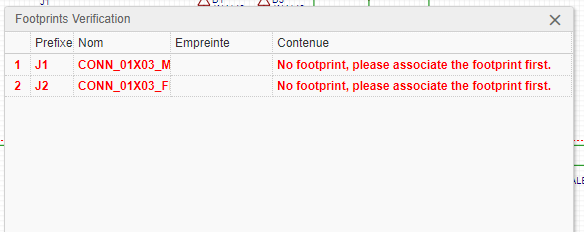
Un composant dans le schéma est représenté par un symbole.
Chaque symbole du schéma doit avoir une empreinte pour le représenter dans le PCB afin que les broches du symbole puissent être correctement mappées sur les plots de l'empreinte et que la connectivité du schéma soit correctement reproduite dans le PCB.
Le symbole dans le schéma doit avoir une empreinte qui lui est attribuée avant que le schéma puisse être converti en PCB.
Les empreintes sont attribuées aux symboles à l'aide du gestionnaire d'empreintes.
Le gestionnaire d'empreintes s'ouvre en cliquant sur l'attribut Footprint du symbole sélectionné dans le panneau de droite.
Veuillez essayer d'utiliser des symboles auxquels des empreintes ont déjà été attribuées dans la bibliothèque.
Vérifiez toujours les symboles et leurs empreintes attribuées par rapport aux fiches techniques du fabricant d'origine.
Vérifiez les correspondances entre les symboles et les broches de l'empreinte et les dimensions de l'empreinte.
Lisez s'il vous plaît:
[https://easyeda.com/forum/topic/How-to-ask-for-help-and-get-an-answer-71b17a40d15442349eaecbfae083e46a](https://easyeda.com/forum/topic/How-to-ask-for-help-and-get-an-answer-71b17a40d15442349eaecbfae083e46a)
A component in the schematic is represented by a Symbol.
Each symbol in the schematic has to have a footprint to represent it in the PCB so that the pins on the symbol can be correctly mapped to the pads on the footprint and the connectivity of the schematic correctly reproduced in the PCB.
The symbol in the schematic must have a footprint assigned to it before the schematic can be converted to a PCB.
Footprints are assigned to symbols using the Footprint Manager.
The Footprint Manager is opened by clicking on the Footprint attribute of the selected symbol in the right hand panel.
Please try to use symbols that already have footprints assigned to them in the library.
Always check the symbols and their assigned footprints against the original manufacturer's datasheets.
Check symbol to footprint pin mappings and footprint dimensions.
Please read:
[https://easyeda.com/forum/topic/How-to-ask-for-help-and-get-an-answer-71b17a40d15442349eaecbfae083e46a](https://easyeda.com/forum/topic/How-to-ask-for-help-and-get-an-answer-71b17a40d15442349eaecbfae083e46a)
Our website uses essential cookies to help us ensure that it is working as expected, and uses optional analytics cookies to offer you a better browsing experience. To find out more, read our Cookie Notice


 Brand new interactions and interfaces.


 Easy to use and quick to get started.