I've got a 4 layer design and want to add stitching vias to the copper areas. I try to use the Add/Rmove Vias function but it doesn't add any vias. Am I not using this feature correctly or is it a bug?
Thanks,
Colby
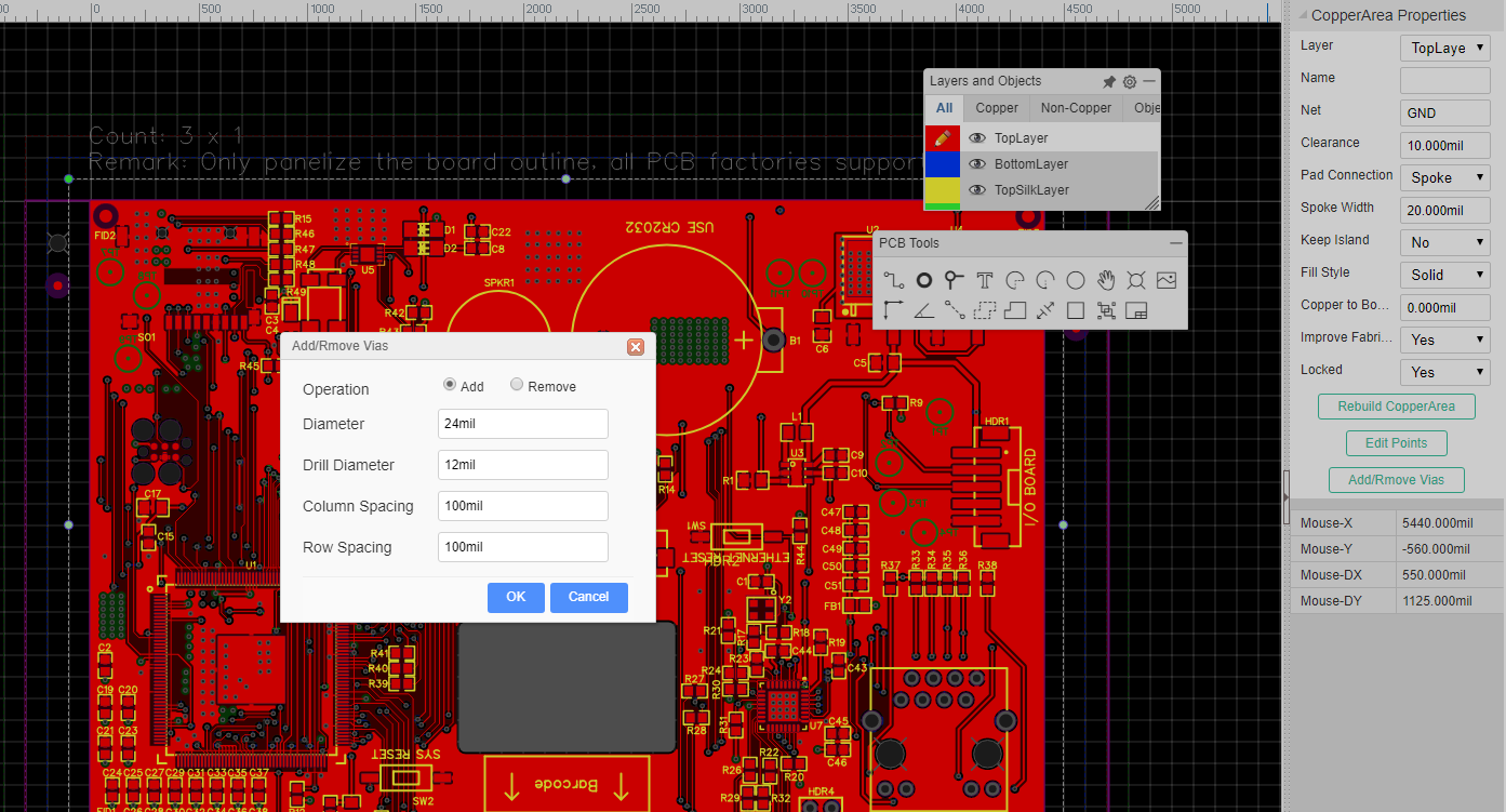
Selecting top copper area (GND) and clicking add vias
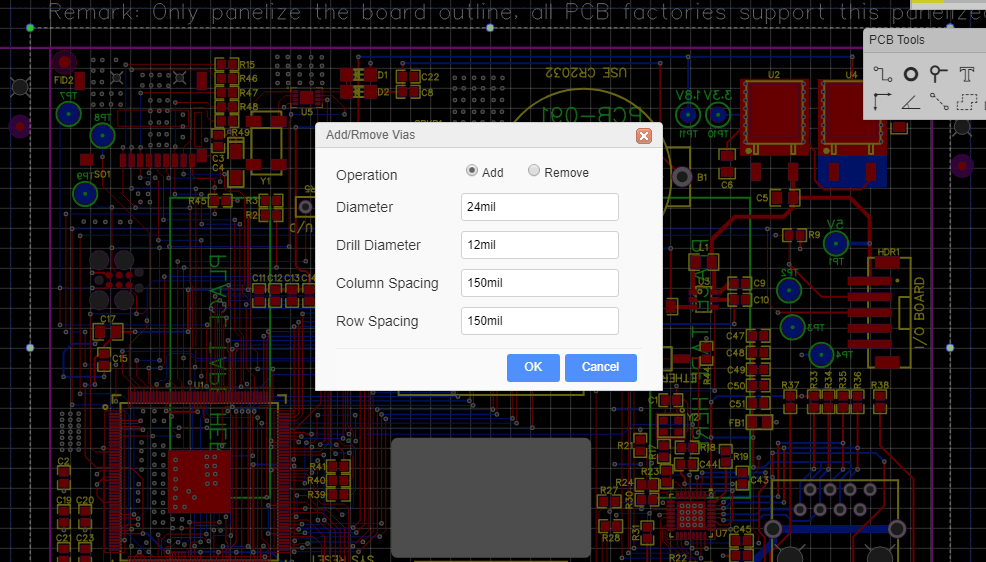
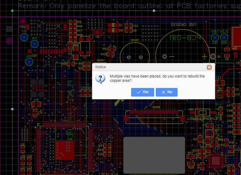
It says multiple vias have been placed, but none have been actually placed
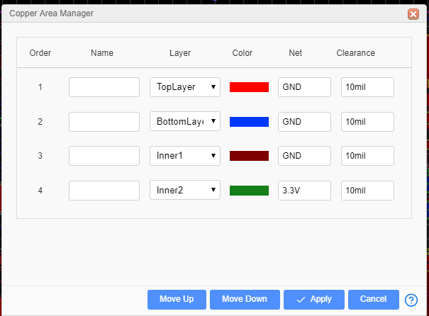
My copper area manager, showing that the top is GND, bottom is GND, Inner1 is GND and Inner2 is 3.3V
@cjohnson , @UserSupport,
I think this is the same issue as originally posted about here:
[https://easyeda.com/forum/topic/Add-vias-to-copper-areas-on-multilayer-board-98e0cdee4bab48fa92c1067d277f6782](https://easyeda.com/forum/topic/Add-vias-to-copper-areas-on-multilayer-board-98e0cdee4bab48fa92c1067d277f6782)
which was also about vias not being added to a 4 layer board.
I did not do a very good job of investigating the issue in that topic because I got sidetracked by the design rather than addressing the original question.
:)
@andyfierman Okay, I don't have time today but I should next Monday to put together an example project that duplicates this issue. This project cannot be made public as it's an actual product unfortunately. I've seen this issue on all of my board designs lately.
This board (ironically because of the original post that had design issue) was made 4 layer due to FCC testing failure in the high frequency RF radiation range. With the amount of components on the board the ground plane is way too chopped up to work as a 2 layer design (I mean it works, but it wont pass FCC). 4 layer fixed the issue, so now I just want the layer stitching to look nice! I have gotten the via placement to work on another 4 layer board but I cannot figure out how to make it work on any other designs.
It looks so nice when the add via function actually works!
@andyfierman My current thoughts are that if the planes are not connected together the add via function will work, but if the planes are already connected together in anyway shape or form it doesn't add anything.
Again, I will create an example project next Monday.
@UserSupport Top, bottom and inner 1 are all GND net. Please read my OP carefully.
I made the copper visible and tried again, but same result.
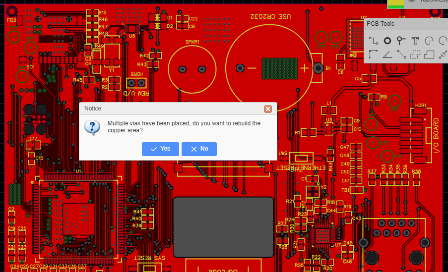
Still shows the same message but no vias were placed.
@UserSupport @andyfierman I'm putting together an example project right now. Took a little more effort to find some free time this afternoon, but I'm letting the autorouter run right now so that the board isn't empty. Not sure how long it takes since I've never used it before.
@UserSupport @andyfierman
Had to open another bug report for the autorouter, but it turns out it wasn't necessary to route anything and duplicate the issue.
Here's a project with a mild amount of components, no traces, but identical planes to my other project. Attempting to add stitching vias does nothing, just says it adds them, but nothing is added.
[https://easyeda.com/cjohnson/viaplaceproject](https://easyeda.com/cjohnson/viaplaceproject)
@UserSupport,
"You need to delete inner layer copper first or set it to GND..."
To clarify what your last post means.
Suppose that I want to join the GND copper by adding add vias to a 4 layer PCB with:
Top layer: GND (Copper Area)
Inner 1: GND (Copper Area or set to PLANE)
Inner 2: VCC (Copper Area or set to PLANE)
Bottom layer: GND (Copper Area)
* Does your last post mean that I should:
1. delete the Inner 2 layer VCC plane (or set it to GND);
2. add the GND vias and then;
3. add the layer 2 VCC plane back in again (or reset it from GND back to VCC)?
@andyfierman Yep....that's exactly what @UserSupport meant
That seams like a definite bug. Not straight forward or documented enough.
Having just spent most of the morning trying to work out why no vias were appearing on my very similar-sounding 4 layer board, I found this topic and used this workaround, which worked. Please fix this bug.
Our website uses essential cookies to help us ensure that it is working as expected, and uses optional analytics cookies to offer you a better browsing experience. To find out more, read our Cookie Notice


 Brand new interactions and interfaces.


 Easy to use and quick to get started.