Are the cutouts located next to the edge connector cut out by JLCPCB when manufactured?
Without sight of your project, it is not clear how those grey rectangles are made.
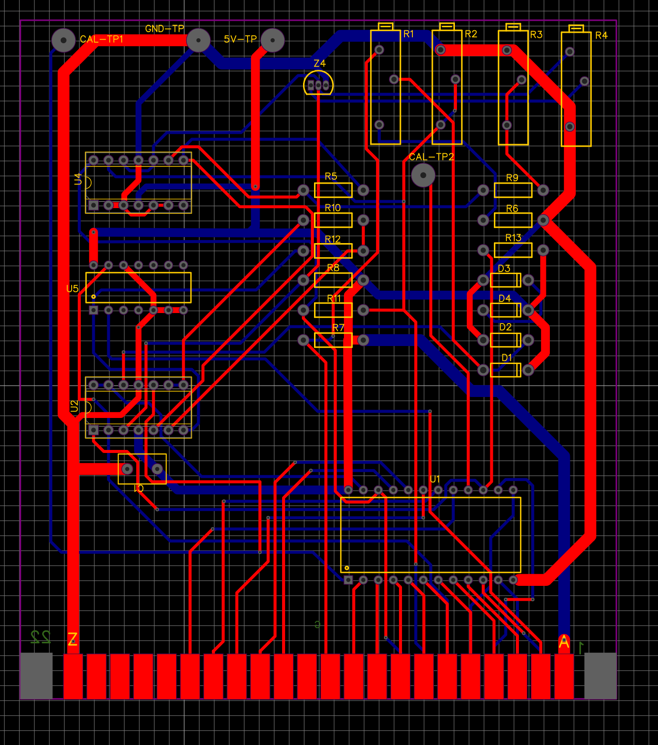
Generate the Gerbers and, using gerbv, check to ensure that those grey rectangle are converted into bits of PCB that are not there.
If not, redraw the board outline to create them explicitly or place Solid Regions set to Cutout.
I am trying to create the cutouts and wondering if JLCPCB actually does cut them out?
I created them by using the Rec tool and then under Solid Region "Type" to the right I selected Board Cutout. Would this accomplish the task?
I would love to be able to use derbv but have already spent a complete day trying to install it. Seems to be beyond my skill level at the moment. Maybe there is an easier way that I have not found.
I gave the Gerber viewer online a try but I didn't see an indication of the cutouts. When I was exporting the Gerber file I noticed they were cut out on the EasyEDA viewer. So I suppose they are. I was just not sure the manufacture would cut them out. I'll find out.
Thanks again for your help, Andy. I only wish I would have discovered this years ago. All my PCB's for my home automation system designed 25 years ago were originally hand wire wrapped. I'm enjoying converting them over to new PCB's and adding a few new modifications. I added a humidity sensor to the last one and looked wonderful. Fun stuff!


Old and new:


To be sure that the cutouts are correct you could redraw the board outline to include them. Then you can be certain the board will have the right shape.
Looks like you are having fun revisiting your designs and are getting the hang of using EasyEDA.
You haven't missed so much because EasyEDA only really became wider known around 2013. There were many other free EDA tools available before then but the big differences were how much easier it was to learn and how it gave cheap access to professional quality PCBs.
What I find to outline the PCB is this:
<br>

Is there a free form option?
Yes, you can draw the outline using the Trace tool but placed in the Board Outline layer.
You can then specify start and end XY points to ensure that the outline is exactly correct and closed.
You can add rounded corners using the Arc tool and specifying start and end XY points
I haven't got a PC handy at the moment to check and I can't remember in detail but you may be able to start with a Solid Region set to Cutout and use the Edit Points tool and then place that into the Board Outline layer. That also allows you to add rounded corners.
A couple of great takeaways from this: Use the track and arc tool to draw the outline, turn off gridlock to finally match arc's and best of all with gridlock off you can jog the line or arc.
I'll be curious to see these small arcs in the finished product.
Our website uses essential cookies to help us ensure that it is working as expected, and uses optional analytics cookies to offer you a better browsing experience. To find out more, read our Cookie Notice


 Brand new interactions and interfaces.


 Easy to use and quick to get started.