Hi, for some reason the DRC thinks that some of the pins on U2 are incorrect. it looks ifne on the schematic. whats going on? - [https://easyeda.com/gonadgranny/open-circuit](https://easyeda.com/gonadgranny/open-circuit)
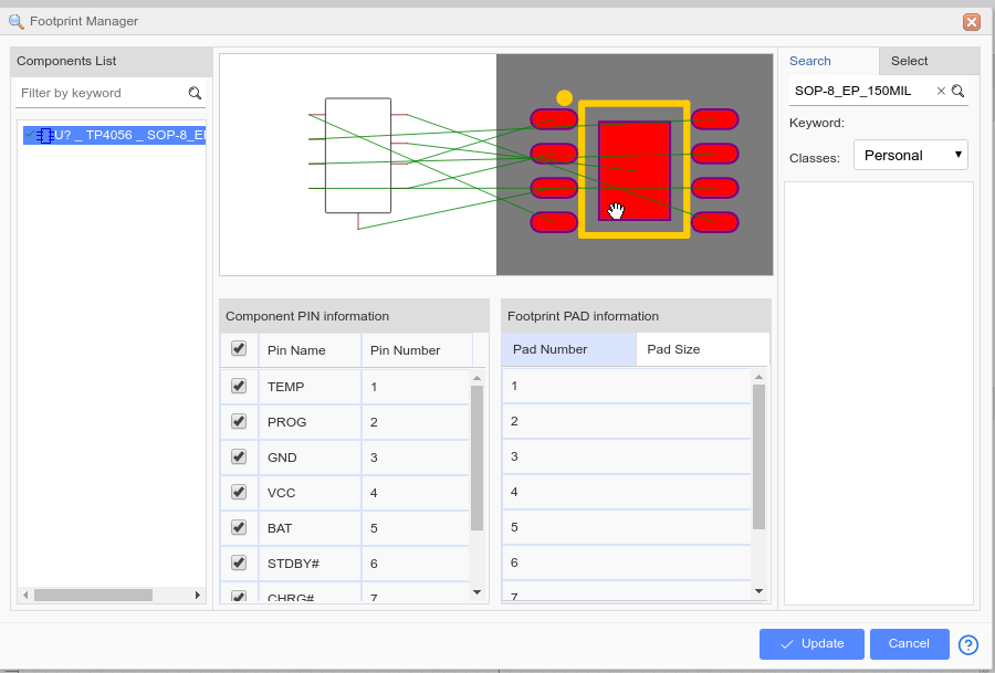
Check that the Schematic Symbol pin to PCB Footprint pad mapping is correct.
Check that the PCB Footprint does not have net names pre-assigned to pads in the Footprint itself.
If it does and it is a System PCB Lib then please report it as an error.
The reason you have DRC errors is because - for whatever reason - you have tracks to the PCB which have different netnames from thosetracks and pads to which they connect.
You should not edite netnames of tracks in the PCB. Edit the connectivity in the Schematic and then do **Update PCB...** and then redraw the tracks as required.
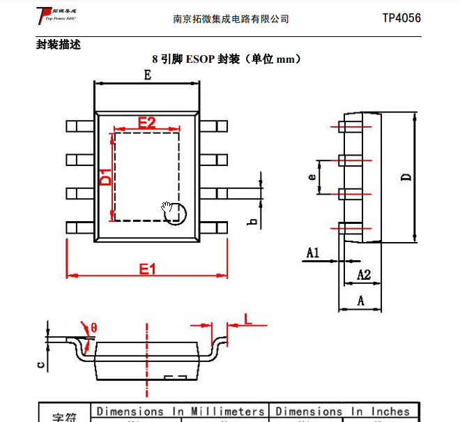
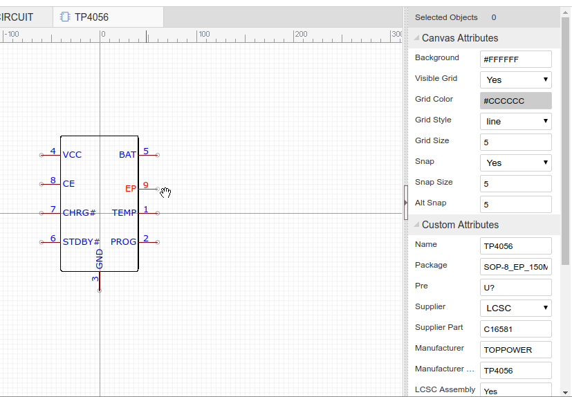
There is also a problem that problem is that the symbol that you have used has no pin 9 for the extended/thermal pad on the bottom of the package.
Please study the datasheet for this part:
[https://lcsc\.com/product\-detail/PMIC\-Battery\-Management\_TP4056\_C16581\.html](https://lcsc.com/product-detail/PMIC-Battery-Management_TP4056_C16581.html)
at:
[https://datasheet\.lcsc\.com/szlcsc/1906261508\_Nanjing\-Extension\-Microelectronics\-TP4056\-42\-ESOP8\_C16581\.pdf](https://datasheet.lcsc.com/szlcsc/1906261508_Nanjing-Extension-Microelectronics-TP4056-42-ESOP8_C16581.pdf)
For the LCSC part C16581, this is the part you should be using:
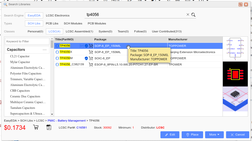
This us what it should be like:
thanks very much for that. on my circuit the pad is connected to ground but the editor is not telling me that it should be connected to ground, why might this be? thanks.
Our website uses essential cookies to help us ensure that it is working as expected, and uses optional analytics cookies to offer you a better browsing experience. To find out more, read our Cookie Notice


 Brand new interactions and interfaces.


 Easy to use and quick to get started.