Schematic View:

Exported PDF - Same area.

I have emailed the json file to the address you supplied.
I'd like to add further, that I have:
1) Removed the X's on three more circuits.
2) Saved schematic
3) Closed Schematic
4) opened schematic
5) Added X's back to the the three circuits affected in #1 above.
6) Saved schematic
7) closed schematic
8) opened schematic
9) exported to pdf.
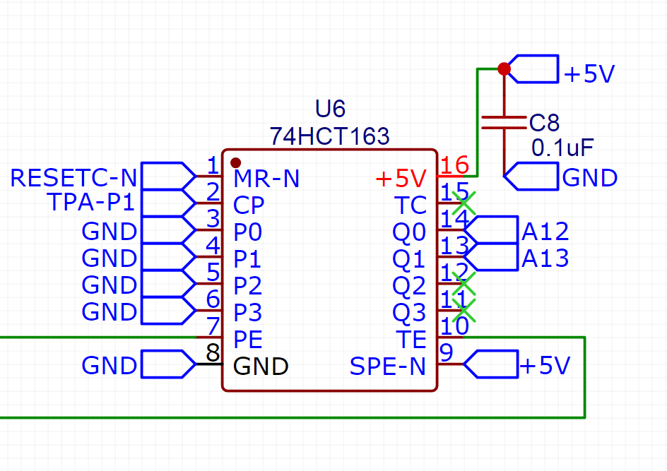
Those three connections now show the same effect:
Notice, on the same schematic, this IC as to how it appears on the PDF:
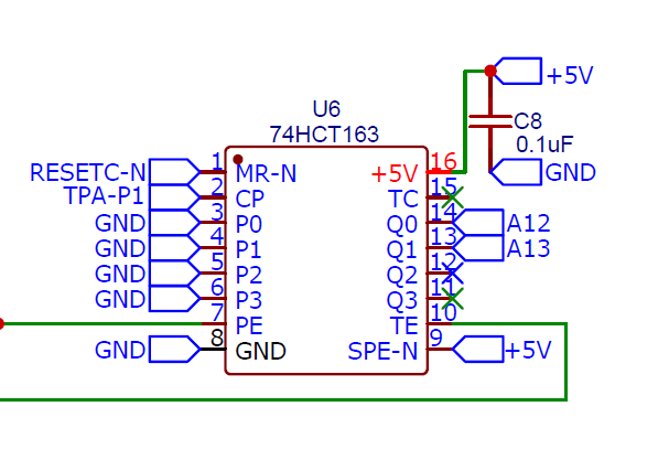
Notice above how on pin 12, it's a blue X, on pin 11, it's a green X. I can assure you that in the schematic view itself, they are both green:
Our website uses essential cookies to help us ensure that it is working as expected, and uses optional analytics cookies to offer you a better browsing experience. To find out more, read our Cookie Notice


 Brand new interactions and interfaces.


 Easy to use and quick to get started.