You need to use EasyEDA editor to create some projects before publishing
Heat Vias and an invisible Copper Pour
2166 29
JulesP 3 years ago
Hi there, 
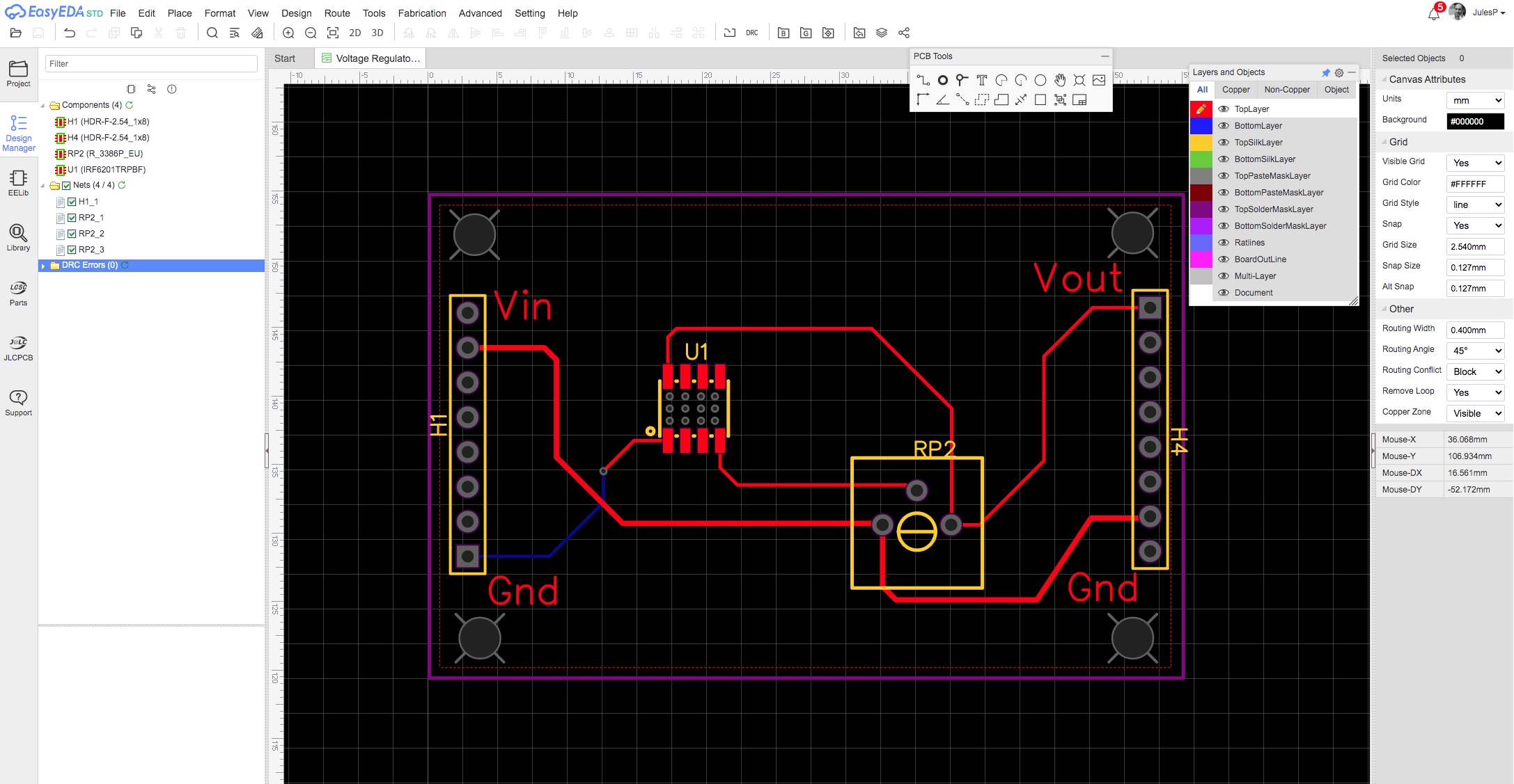
I have a query about the best way to assist heat transfer away from a MOSFET that is likely to get quite hot. The simple circuit involves an IRF6201 with its small SOIC-8 package with which I will add a heat sink on top. However, I also wish to add some vias within the area of the footprint, as can be seen in the image. My approach is to lay out a grid of 9 vias within the main IC footprint and then do a GND Copper Pour which should allow heat to flow from the underside of the chip to the large copper area. Firstly, when I did the Copper Pour I could not get it so show despite it being 'Visible' so it's hard to see the interaction with the vias. Secondly, is this the simplest way to assist heat transfer or should I add instead a Pad under the chip and put vias in that? I have read various forum posts on the topic but I end up being a little confused by all the detail. Thanks ![Voltage Reg 1.jpeg](//image.easyeda.com/pullimage/xN7gVeOIbroMrZiMpzdEyKluntrHM8QUgS7Hae1a.jpeg)
Comments
andyfierman 3 years ago
Please see: [https://easyeda.com/forum/topic/How-to-place-multiple-vias-in-a-PCB-footprint-a34cf68d58414138898a56de60abd8c1](https://easyeda.com/forum/topic/How-to-place-multiple-vias-in-a-PCB-footprint-a34cf68d58414138898a56de60abd8c1)<br> <br> Your Copper Area will only fill if there is something inside its boundary with the same netname as that assigned to the area.
Reply
JulesP 3 years ago
Thanks for the link. I realised the issue with the lack of the Gnd net in the night but thanks for confirming it. J
Reply
Markus_ee 3 years ago
Hi! Check out Daves videos on the subject in the EEVblog: [https://www.youtube.com/watch?v=2ygnAv6koSQ&t=0s](https://www.youtube.com/watch?v=2ygnAv6koSQ&t=0s)<br> <br> [https://www.youtube.com/watch?v=q3RhWuXFixU](https://www.youtube.com/watch?v=q3RhWuXFixU)<br> <br> Regards, Markus Virtanen HW / Electronics Designer
Reply
andyfierman 3 years ago
@JulesP, @markus_jidoka, I have just updated: [https://easyeda.com/forum/topic/How-to-place-multiple-vias-in-a-PCB-footprint-a34cf68d58414138898a56de60abd8c1](https://easyeda.com/forum/topic/How-to-place-multiple-vias-in-a-PCB-footprint-a34cf68d58414138898a56de60abd8c1)<br> <br> To add: [https://easyeda.com/forum/topic/How-to-remove-the-exposed-copper-close-the-solder-maks-aperture-in-a-through-hole-pad-5673aa46a6a34172ae2ad9ade57aaa87](https://easyeda.com/forum/topic/How-to-remove-the-exposed-copper-close-the-solder-maks-aperture-in-a-through-hole-pad-5673aa46a6a34172ae2ad9ade57aaa87)<br> <br> (for "maks", please read "mask" but I can't be bothered to go back and repost the whole topic just to correct the typo in the url...)
Reply
JulesP 3 years ago
So to try and summarise the various contributions, I should use a pad instead of vias under the IC footprint on both layers. Should I then connect them together with a hole of some sort?
Reply
Markus_ee 3 years ago
Hi JulesP! Vias are always a good way to heatsink your MOSFET heat to ground. But let me just say that there are so many heatsinking solutions out there and they all depends on the specs what you have set into your project. All I can give is a few good examples in my projects: [https://easyeda\.com/markus\_jidoka/li\-ion\_solar\_charger\_pcb1\_v3\-0](https://easyeda.com/markus_jidoka/li-ion_solar_charger_pcb1_v3-0) [https://easyeda\.com/markus\_jidoka/400v\_geiger\_tube\_psu\_v1\-0\_copy](https://easyeda.com/markus_jidoka/400v_geiger_tube_psu_v1-0_copy) [https://easyeda.com/markus_jidoka/TP4056-750mA-03962A-Lithium-Battery-Charger-Module-v2.0](https://easyeda.com/markus_jidoka/TP4056-750mA-03962A-Lithium-Battery-Charger-Module-v2.0) [https://easyeda\.com/markus\_jidoka/li\-ion\_solar\_charger\_pcb2\_v3](https://easyeda.com/markus_jidoka/li-ion_solar_charger_pcb2_v3)<br> <br> And if you want, I can be "hired" to do the professional layout/schematic for you. I always have spare time on weekends... Regards, Markus Virtanen HW / Electronics Designer
Reply
andyfierman 3 years ago
@JulesP, Vias cannot be assigned pad numbers so if you include them in a footprint they will create avoid DRC errors. There is no control over the solder mask coverage of a via. Therefore to avoid DRC errors in a footprint and o give you control over what copper areas are exposed or not, it is best to use pads. If you are using them in a more general context of a layout and not as part of a footprint then using vias may or may not better suit your purposes.
Reply
JulesP 3 years ago
Hi Andy, Ive accepted that I will need to use a Drain Pad within the footprint of my single MOSFET and on both layers so my further query was whether vias scattered over that area are the best way to conduct heat down between the top and bottom pad. I’m assuming they are. jules
Reply
JulesP 3 years ago
When I’ve made the changes I will post it up here 😊
Reply
JulesP 3 years ago
@markus_jidoka Thanks but I’m not looking to hire someone but rather learn as I go along with the various aspects of my project work.
Reply
JulesP 3 years ago
Ok, my attempt at symbol and footprint modification is going only half ok. I have followed the steps to do this but when I try and link the two files together it doesn't stick despite saying that it has updated it. So in the two attached grabs, the first is the linking of the cloned schematic symbol with the edited footprint and which I then update. However, when I reinstall the schematic component it shows the 'old' footprint. I expect it's something very simple but I can't see it - may be to do with the Class it's saved in? Thanks for your patience. ![Component Customisation 1.jpeg](//image.easyeda.com/pullimage/MYircCAT1DgDVzY1KUL3R0UyWnC0lwofW9U3elJG.jpeg) ![Component Customisation 2.jpeg](//image.easyeda.com/pullimage/YDUpZdVSnfh00yFkeFX476LyvSTs1Wk74UrYgbDz.jpeg)
Reply
andreasbernhofer 3 years ago
@JulesP In the library view, right-click the footprint and hit "refresh", that may help.
Reply
JulesP 3 years ago
Thanks. I did it in the end but it wasn't helped by refresh but instead setting the tags on the 'Select' menu in the Footprint manager to All(My Libraries). No idea why but it comes up correct now. However, a DRC error shows saying that the central pad is too close to one of the chip pads. Why only the first pad and not the rest in that row and how can I maintain contact with the Drain pins for heat transfer without getting this error? ![DRC Error.jpeg](//image.easyeda.com/pullimage/uRFTSoJEhN6jtVt8pRhAwMfF4ZszHqyVEm5vfF5m.jpeg)
Reply
andyfierman 3 years ago
@JulesP, See UserSupport's comment in this Bug Report: [https://easyeda.com/forum/topic/New-Footprint-NOT-registering-a961a0ca381e498d9d5097c6bbfc3604](https://easyeda.com/forum/topic/New-Footprint-NOT-registering-a961a0ca381e498d9d5097c6bbfc3604)
Reply
JulesP 3 years ago
Hi Andy, Thanks, I have found my way through that issue, but a different one remains. How do I avoid DRC errors to do with clearance between my heat sink pad and the Drain pins? I thought it might be because I had not specified the Drain pads as being electrically connected to the central heat sink pad so I revised the symbol (Pic 1), the footprint (Pic 2) and the circuit (Pic 3) to do that but I still get tolerance errors (Pic 4). Am I doing this completely the wrong way? J ![Pic 1.jpeg](//image.easyeda.com/pullimage/yhjTN3WQ9trRh9AMV3EZJkFnOkNPDcLfIRszEFNG.jpeg) ![Pic 2.jpeg](//image.easyeda.com/pullimage/hyimDelxQlZoeztYtUnBznB9Os6DW0sBaR7nBhii.jpeg) ![Pic 3.jpeg](//image.easyeda.com/pullimage/5auxaAOlVamyt71DXJz3AnpZvjhHxYw3yIesBdlI.jpeg) ![Pic 4.jpeg](//image.easyeda.com/pullimage/cXwlYsHcPehoNRpQDGzasHyeZ0FXyx5erodAgJ0T.jpeg)
Reply
andyfierman 3 years ago
The problem here is that you cannot short pads with different numbers together. * The schematic symbol represents the electrical functionality and connectivity in terms of nets of the device. It does not represents it's physical packaging. Please see: [https://easyeda.com/forum/topic/How-to-avoid-DRC-errors-when-connecting-to-PCB-Footprints-a-k-a-PCB-Libs-90bf944fe3644b21a7d27a9e9d8df8d6](https://easyeda.com/forum/topic/How-to-avoid-DRC-errors-when-connecting-to-PCB-Footprints-a-k-a-PCB-Libs-90bf944fe3644b21a7d27a9e9d8df8d6)<br> <br> In your case the symbol should just show a 3 pin MOSFET with one drain, one gate and one source pin numbered for example as: D=1 G=2 S=3 The Footprint should have 9 pads as you have shown but there should be one gate pad numbered 2, three source pads numbered 3 and four drain pads plus the thermal pad numbered 1. For more on this please see (2.2) and (2.3) in (2) in: [https://easyeda.com/forum/topic/How-to-ask-for-help-and-get-an-answer-71b17a40d15442349eaecbfae083e46a](https://easyeda.com/forum/topic/How-to-ask-for-help-and-get-an-answer-71b17a40d15442349eaecbfae083e46a)
Reply
andyfierman 3 years ago
My comment: "The schematic symbol represents the electrical functionality and connectivity in terms of nets of the device. It does not represents it's physical packaging." is my opinion as a professional engineer. There are a huge number of symbols in EasyEDA that do not conform to this philosophy. This is because of the belief that it is easier for educational and hobbyist purposes to show a symbol that resembles the physical package and pinout so that there is a closer mapping of the schematic and the PCB layout. Whilst this is true, it creates the kind of problems that this post very clearly illustrates and is why professional EDA tools do not do this. In particular, this approach teaches very bad habits for students wishing to progress on to professional positions and using other commercial EDA tools.
Reply
JulesP 3 years ago
Thanks Andy. I will take some time to fully digest this.
Reply
JulesP 3 years ago
Andy, I can appreciate the idealogical issue around the symbols' representation. I have now done what you suggest and have got all the errors to go. I'm assuming that vias are essential to connect the thermal pads on both layers together and have included nine of those, associated with the Drain pins. ![Pic 1.jpeg](//image.easyeda.com/pullimage/OYZsHT7MhbY4uREiNWO6HrBP0MWdgdpmO72gKWTr.jpeg)
Reply
andyfierman 3 years ago
Twelve? :) Yes, the "via" pads are to reduce electrical and thermal resistance between the top and bottom (and any inner layers on 4 or more layer boards). The datasheets and apps notes for this sort of thermal padding is very poorly documented so it is guesswork about what size and how many thermal vias there should be. I have not found a calculation for thermal vias. One point though is that for thermal use at least, they should be filled with solder which means that there should be extra solder paste to fill them or that the "vias" should be exposed on the opposite side of the board from that which the component is mounted on as well as on the component side to allow a second pass of soldering to fill them from the side opposite to that which the component is mounted on.
Reply
andyfierman 3 years ago
You may need a second hand soldering pass anyway as I have no idea how pcb manufacturers scale the solder deposits for multiple "vias in pads to account for the solder that will be "theived" by the through plating anyway. Detailed questions for JLCPCB or whoever is grabbing your boards. One thing I have done with a few TO220 and DPAK footprints for hand soldering is to put a single large hole through the pads that I can then get a soldering iron tip into to flood the hole and the joint face between pad and tab with solder. It also makes it easier to reworking if you have no hot plate, small nozzled heat gun or dedicated desoldering tools or workstation.
Reply
JulesP 3 years ago
Yes, I guess I’ve been a bit zealous but, based on the Spice simulation for heat dissipation shown below, this poor little chip could need to handle 150W when it’s losing 6V at over 20A. Would another/additional option be to do a Copper Pour based on the RP2_1 net instead of Gnd? Then heat can also have a large surface area to dissipate from that is directly connected to the Drain and its 4 pads. There are no HF issues to deal with that might benefit from having a GND Copper Pour. I will write to JLCPCB re vias (maybe just 5 instead of 12) and post their reply. Jules ![IRF6201.jpg](//image.easyeda.com/pullimage/bi3OzW7lqmC68zuvgNEVqkLYQSXVQWJIUcAbeAWU.jpeg)
Reply
andyfierman 3 years ago
@JulesP, Bear with me... * The issues that appear from your LTspice sim ask different questions from those of the Footprint and thermal vias etc. 1. Do you have a some sort of a Design Requirement Specification that defines what you are trying to achieve with the circuit in your sim? 2. Is that the same circuit as in your EasyEDA project? The reason I ask is that from the Infineon datasheet the IRF6201 is not suitable simply because it has a max power dissipation of 2.5W when mounted on 1 inch square copper board: [https://www.infineon.com/dgdl/irf6201pbf.pdf?fileId=5546d462533600a4015355e4445919ce](https://www.infineon.com/dgdl/irf6201pbf.pdf?fileId=5546d462533600a4015355e4445919ce)<br> <br> You can increase the board area and add more layers to via together but unless you have forced air or liquid cooling there is no way you can get enough heat out of that package to allow it to dissipate 150W. For gate voltages above about 7.35V (104.5degrees pot rotation), you also way exceed the absolute maximum 27A drain current. Increasing the copper area offers diminishing returns since the extra area is further away from the heat source. The heat has to conduct through the smaller area nearest to the device before it can spread out into the wider area so the area around the chip heats up more: very roughly in inverse proportion to the area. * I'm not sure JLCPCB will be able to offer advice about vias sizes and numbers but, I have just found this from TI: Application Report SNVA419C–April 2010–Revised April 2013 AN-2020 Thermal Design By Insight, Not Hindsight [https://www.ti.com/lit/an/snva419c/snva419c.pdf](https://www.ti.com/lit/an/snva419c/snva419c.pdf)<br> <br> You have also said that "There are no HF issues to deal with that might benefit from having a GND Copper Pour." which also implies that this is not part of some sort of switching regulator where the MOSFET is only dissipating power when fully on or fully off or is only switched partly on for a very short period. * Sorry but with my current understanding of you aims: your circuit as it stands is not going to work. With that in mind, if you do feel that you would like more detailed design help with your project, please feel free to PM myself (or through enquiries at signality.co.uk) or Markus. :) <br> <br>
Reply
andyfierman 3 years ago
@JulesP, Forgot to add: ![image.png](//image.easyeda.com/pullimage/Fw0NSNHSsr2bogCg4EkUv884IXFCKTJHQhvm0PHY.png)
Reply
JulesP 3 years ago
Hi Andy, I have had a reply from JLCPCB which says: "These thermal vias for exposed pads are quite common in PCB design (for SOIC and QFN packages). Just use via with the smallest drill size (0.3mm dia), it will be OK. You don't need to fill the vias. Please read page 8 of [https://www.nxp.com/docs/en/application-note/AN2409.pdf](https://www.nxp.com/docs/en/application-note/AN2409.pdf)<br> <br> If you search pcb thermal via you can see more application notes on this." I will drop you a line regarding my project. Jules
Reply
JulesP 3 years ago
![0AB798BE-69DA-4271-B32E-0E6FD96884F3.png](//image.easyeda.com/pullimage/UgFtoVYSj7oi26agXXynNgEeYOMMG1V3SJ72D5n4.png)Upon reflection my 12 vias is very reasonable 😊
Reply
andyfierman 3 years ago
@JulesP, @JLCBPCsupport, That's very useful info from JLCPCB. It would be good if JLCPCB could add this kind of information and notes on their Capabilities page. :) There is a bit about plating of vias in 3.2.1 Example: Thermal Impedance of VIA Array on page 7 of: [https://www.ti.com/lit/an/snva419c/snva419c.pdf](https://www.ti.com/lit/an/snva419c/snva419c.pdf)
Reply
Login or Register to add a comment
goToTop
你现在访问的是EasyEDA海外版,建议访问速度更快的国内版 https://lceda.cn(需要重新注册)
如果需要转移工程请在个人中心 - 工程 - 工程高级设置 - 下载工程,下载后在https://lceda.cn/editor 打开保存即可。
有问题联系QQ 3001956291 不再提醒
svg-battery svg-battery-wifi svg-books svg-more svg-paste svg-pencil svg-plant svg-ruler svg-share svg-user svg-logo-cn svg-double-arrow -mockplus- -mockplus- -mockplus- -mockplus- -mockplus- -mockplus- -mockplus- -mockplus-@1x -mockplus-

Cookie Notice

Our website uses essential cookies to help us ensure that it is working as expected, and uses optional analytics cookies to offer you a better browsing experience. To find out more, read our Cookie Notice