You need to use EasyEDA editor to create some projects before publishing
Help needed with NRF24 reference design
1256 21
Bob Kruijer 3 years ago
Hi, 
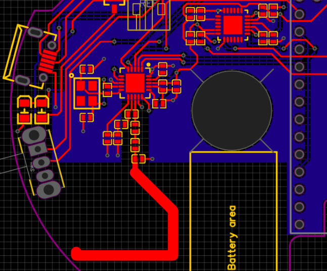
I had a question about one of my earlier PCB design based on the NRF24L01+ wireless transceiver.  This was a correct schematic, but the PCB design was not 'reference' and did not give a good signal, it was noisy and had dropouts. Based on feedback on this forum I concluded I best go with a reference design from the manufacturer. I have now done that and got some boards made. The layout is pretty much exact what the manufacturer recommends, but now I do not get any signal at all, but the chip does initialize properly. Any ideas on how to troubleshoot this?  Here is my pcb design, and below I'll paste the manufacturer reference design. ![image.png](//image.easyeda.com/pullimage/ksPMY2NuBZWgjTXCduuZ0Cgjcf0qbkmboQK9xq4v.png) ![image.png](//image.easyeda.com/pullimage/3pA69Oot5uZDz1f7Ektxxiw77nxDxB5tQbqNvj4d.png) 
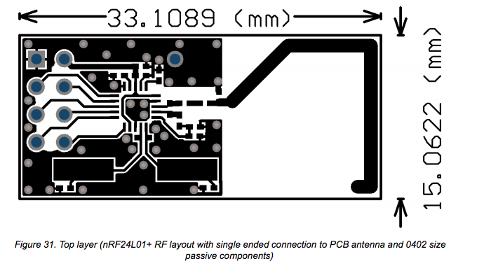
I have been reading up a bit about antenna design and fro what I gather the single ended antenna should be more forgiving than a MIFA (which I had before). I'm kinda stumped on where to go from here... Tia for any guidance on troubleshooting.
Comments
andyfierman 3 years ago
Can you make your project public?
Reply
andyfierman 3 years ago
Can you also post the link to the earlier topic in the forim to avoid having to go over old ground? Thanks.
Reply
andyfierman 3 years ago
Also, please post a link to the manufacturer's recommendations and reference design that you have used.
Reply
Bob Kruijer 3 years ago
Hi Andy, thanks for your comments so far. I have made a version public here [https://oshwlab.com/project/publish/c239cd6eee56430faf81d7f8891b76ac](https://oshwlab.com/project/publish/c239cd6eee56430faf81d7f8891b76ac)<br> <br> This is the old topic: [https://easyeda.com/forum/topic/PCB-antenna-trace-impedance-9ba58ee6474c4edda01052b4e9e99170](https://easyeda.com/forum/topic/PCB-antenna-trace-impedance-9ba58ee6474c4edda01052b4e9e99170)<br> <br> This is the datasheet, page 65 has the layout I tried to copy [https://www\.sparkfun\.com/datasheets/Components/SMD/nRF24L01Pluss\_Preliminary\_Product\_Specification\_v1\_0\.pdf](https://www.sparkfun.com/datasheets/Components/SMD/nRF24L01Pluss_Preliminary_Product_Specification_v1_0.pdf)<br> <br> Regards, Bob
Reply
andyfierman 3 years ago
@b.kruijer, Sorry Bob but that's not the right link to view your oshwlab page. Please check this topic: [https://easyeda.com/forum/topic/How-to-make-a-Project-public-and-share-the-links-to-it-9f006513b84b412580910905b0281d20](https://easyeda.com/forum/topic/How-to-make-a-Project-public-and-share-the-links-to-it-9f006513b84b412580910905b0281d20)
Reply
Bob Kruijer 3 years ago
@andyfierman oh wow, didn't know that link sharing was broken. How about this one: [https://easyeda\.com/editor\#id=\|2eecd3cf8f844832a3b4728ce44df64a\|da6b9e992fe44f0bb6fb659b59cead3f\|5996d69a56b147f89872242fee77941f\|7df36cc7e35b4246a1cc786eb20f48fc\|7ed1d194f5404c969482ea5118de2929](https://easyeda.com/editor#id=|2eecd3cf8f844832a3b4728ce44df64a|da6b9e992fe44f0bb6fb659b59cead3f|5996d69a56b147f89872242fee77941f|7df36cc7e35b4246a1cc786eb20f48fc|7ed1d194f5404c969482ea5118de2929)<br> <br> Cheers, Bob
Reply
andyfierman 3 years ago
Yes, that works.
Reply
martin 3 years ago
Do you have RF equipment that can help troubleshoot this a little? A simple SDR would do for a start. Also, that antenna will be detuned since your ground plane is not the same as the manufacturer's, but you should still be able to pick up a signal. Thoughts: 1\. Impedance mismatch is too great\, chip resets when you try to transmit \(try lower power transmission\) 2\. HF crystal mounted backwards \(don't probe it\!\)
Reply
andyfierman 3 years ago
@b.kruijer, The antenna trace is not quite the same length at the tip as the reference design but I have no idea how much difference that would make. Could the battery be too close to the antenna? Is the antenna exposed copper? If exposed, is it HASL or ENIG finish? Sanity check: do you have a reference design board from Nordic against which to compare the performance of your board? This is a very good article that may help if you need a respin: [https://colinkarpfinger.com/blog/2010/the-dropouts-guide-to-antenna-design/](https://colinkarpfinger.com/blog/2010/the-dropouts-guide-to-antenna-design/)<br> <br> which includes a link to: [https://www.ti.com/lit/an/snoa519b/snoa519b.pdf](https://www.ti.com/lit/an/snoa519b/snoa519b.pdf)<br> <br> which has a nice explanation of that the antenna is really doing. It is important to realise that antenna design is not about designing a nice 50 Ohm track, which is what some people seem to think is the case. The transceiver end of the antenna has to be impedance matched to the device by some sort of matching network. The rest of the antenna is about matching the antenna copper on the board to the characteristic impedance of free space, which is about 377 Ohms. The biggest take away from the article above is that you need some decent RF test kit. The 2nd biggest take away is that you need to make several boards to characterise the PCB fab process and to try out different antenna designs. An old radio amateur trick was to make the antenna too long then trim bits off the end to tune it up. So, you need several of each to try tweaking them by by cutting away bits of end copper. Note that [https://www.nordicsemi.com/Products/Low-power-short-range-wireless/nRF24-series](https://www.nordicsemi.com/Products/Low-power-short-range-wireless/nRF24-series) is marked as not recommended for new designs. :(
Reply
martin 3 years ago
> The biggest take away from the article above is that you need some decent RF test kit. > The 2nd biggest take away is that you need to make several boards to characterise the PCB fab process and to try out different antenna designs. > An old radio amateur trick was to make the antenna too long then trim bits off the end to tune it up. So, you need several of each to try tweaking them by by cutting away bits of end copper. In terms of kit, you can get by with an SDR and a relatively cheap VNA, for hobby work. I think even a NanoVNA will do to tune an antenna at 2.4 GHz these days. I've gotten excellent results designing boards using a xaVNA (open source) and a PlutoSDR. JLCPCB boards have been working well, as long as I properly tune the antenna with the VNA. I'd rather use some RF caps and inductors than cut up my antennas :-) All this to say, totally doable with minimal monetary investment, and a fair chunk of time for someone only just starting. Ref project: [CC1312 Breakout - EasyEDA](https://easyeda.com/martin/cc1352-breakout_copy) -- I put these guys everywhere as part of a 15.4 network now! <br> <br>
Reply
andyfierman 3 years ago
"I'd rather use some RF caps and inductors than cut up my antennas" The RF caps and inductors match the transceiver to the antenna. Good impedance matching transfers maximum power between the transceiver to and from the antenna. However, unless you can show that this power is actually being radiated (or received from) free space, that doesn't guarantee that the antenna is a good radiator/receiver of RF power. You can design a matching network to match the transceiver to a resistor or a well terminated transmission line neither of which form an efficient antenna. In both cases there can be maximum power transfer but in both cases that power will just be dissipated as heat in a resistance. An inefficient antenna will do the same, it can look like a good impedance match but little power is transferred between it and free space whilst most of it is dissipated as heat in the copper and the substrate. A measurement of how well the antenna resonates is not a good guide either without understanding how much of the measured resonance is in the antenna itself and how much is in the matching network. A nice clean resonance can be obtained in a simple LC circuit but very little energy may be transferred outside of those components. Hence they are useless as an antenna. Unless you can measure the power being radiated by the antenna out into free space and can compare that with how much power is being supplied to it from the transmitter then you have no way of knowing that it's effective as an antenna. Hence the need to make different versions of an antenna and to play about trimming the physical length of the antenna. Then the matching networks can be adjusted and power measurements can be compared. Then, in the absence of any actual radiated power measurements, the assumption made that the combination that transfers the most power for the lowest SWR is actually converging on the most efficient antenna. For more, see Efficiency and Impedance matching in: [https://en.wikipedia.org/wiki/Antenna_(radio)](https://en.wikipedia.org/wiki/Antenna_%28radio%29)
Reply
martin 3 years ago
(OP, derailed the thread a little, sorry) I start with [https://www.ti.com/tool/CC-ANTENNA-DK2](https://www.ti.com/tool/CC-ANTENNA-DK2)<br> <br> But of course, you are right. I was working with the assumption that the antenna is already a good radiator. I think someone wrote spectrum analyzer software for the PlutoSDR. I might get around to buying an attenuator, do some conducted tests, and use the SDR again for radiated energy.
Reply
andyfierman 3 years ago
@martin, @b.kruijer, I didn't know about that antenna kit. It look like a good idea. I didn't mean to sound discouraging but I have seen so many projects here and on other forums where people assume that the antenna as just another bit of wiggly copper track and then come onto forums with questions about poor tranceiver performance. In the early days of Nokia mobile phones, they used to develop a working antenna design on a specified substrate, made in a specified PCB fab house with a specified set of design rules and then nail that fab house to use that substrate with those design rules and no deviations. The rest of the phone assembly was almost an afterthought given the precedence they placed on getting an efficient and repeatable antenna performance. Antenna design is probably the most difficult aspect of PCB design which still really needs a big investment in terms of time, learning, patience and test equipment, well beyond that needed for any other aspect. I think I'd even put it above design for EMC. A colleague many years ago had a phrase that sums stuff like this up nicely: "That is a non-trivial task."
Reply
Bob Kruijer 3 years ago
@martin I tried lower power transmit setting, no difference. ALso, the crystal orientation should not matter afaik? There is no polarity?
Reply
Bob Kruijer 3 years ago
@andyfierman thanks for all the comments and sharing those articles.  I have an RF explorer but no other 'decent' kit to analyze, I think I'll shop around and see what I can get for this purpose. I got some comments from the Nordicsemi dev guys stating that the GND plane was missing on the top side. This is true, as in my layman pcb design mind the GND plane is usually on the bottom and is just 'handy' to via all your GND connections to. I am a bit concerned though as from what I gather I should be able to get 'some' kind of signal, and I don't seem to be getting any, but I'm not sure where to start to troubleshoot this. I've checked the schematic once more against the reference design and it seems to be pretty spot on. The missing GND plane on top should not cause a total collapse of signal. The antenna is exposed copper and is all standard jlcpcb stuff, I believe they typically provide HASL.
Reply
andyfierman 3 years ago
HASL rather unpredictably increases the effective thickness of the antenna. It adds mechanical height but since solder is a much poorer conductor than copper, it probsbly doesn't add as much electrical height. Also, due to the skin effect, the signal will be travelling on the surface of the conductors so that may make the antenna more lossy as well as detuning it. Although more expensive, ENIG may be probably a safer bet. It is much thinner and presents a more conductive gold finish on the exposed side.
Reply
andyfierman 3 years ago
Can you feeds signal directly intobthe receiver to check it out? Have you got an earlier version that is known to work even if not very well?
Reply
andyfierman 3 years ago
The bottom side ground plane is important because it can be made continuous unlike on the component side.
Reply
martin 3 years ago
@b.kruijer The HF crystal has a polarity, so you can't mount it any which way: And at the distances you are presumably testing, I doubt the antenna is the culprit at this stage. ![Screen Shot 2021-03-27 at 5.39.08 AM.png](//image.easyeda.com/pullimage/mbSozPiHuz2ZKjphUgObNay1rYsJemfV1rHLUBnu.png)
Reply
andyfierman 3 years ago
@b.kruijer, **Ah! Just noticed something.** There is what looks like a contradiction in the datasheet about the usage of the central Extended Pad (EP/pin 21) of the Nordic nRF24L01+ chip. Whilst the section 10.4 PCB layout and decoupling guidelines on page 62 of: [https://www\.sparkfun\.com/datasheets/Components/SMD/nRF24L01Pluss\_Preliminary\_Product\_Specification\_v1\_0\.pdf](https://www.sparkfun.com/datasheets/Components/SMD/nRF24L01Pluss_Preliminary_Product_Specification_v1_0.pdf) has a lot of very good layout guidelines, it also says: **The exposed die attach pad is a ground pad connected to the IC substrate die ground and is intentionally _not_ used in our layouts. We recommend to keep it _unconnected_.** Figures 31 and 32 however, clearly show that the central pad as well as pins 8, 14 and 20 are all connected **directly** to the ground plane using vias! ![image.png](//image.easyeda.com/pullimage/O3PY0ccFT4Ig8nBpJMYp6nnLpA460tBVJxLfDB4j.png) You have followed their written advice but not what is shown in their reference design. Personally, I cannot imagine why you would _not_ connect the ground die attach pad of a 2.4GHz trasceiver chip to a very low electrical and thermal impedance ground plane. This and similar posts on the Nordic Dev forum are somewhat belatedly helpful: [https://devzone.nordicsemi.com/f/nordic-q-a/1256/nrf24l01-ground-die-pad](https://devzone.nordicsemi.com/f/nordic-q-a/1256/nrf24l01-ground-die-pad)<br> <br> It implies that they are in fact capacitively coupling the pin21 EP to ground. This would require a carefully constructed footprint for the nRF24L01+ chip which is unlike that created by LCSC since the EP needs to be a pad but also needs to covered by soldermask. There are some recent (lengthy!) posts in the forum about how to do this sort of thing: [https://easyeda.com/forum/topic/Non-exposed-coper-vias-in-footprints-341192f38fb04a1b8addae2065ba400c](https://easyeda.com/forum/topic/Non-exposed-coper-vias-in-footprints-341192f38fb04a1b8addae2065ba400c) or if you want to contact me via signality.co.uk, I would be happy to quote you for constructing a dedicated footprint. <br> **About the crystal: ** To clarify my earlier post: "The bottom side ground plane is important because it can be made continuous unlike on the component side." If you compare your PCB with the reference layouts in Figures 31 and 32 in: [https://www\.sparkfun\.com/datasheets/Components/SMD/nRF24L01Pluss\_Preliminary\_Product\_Specification\_v1\_0\.pdf](https://www.sparkfun.com/datasheets/Components/SMD/nRF24L01Pluss_Preliminary_Product_Specification_v1_0.pdf) you can see that you have removed ground plane from the bottom layer and broken it up with a couple of tracks whilst the top layer is also very busy with lots of tracks and has no ground fill on it. The crystal could be fitted either way round when rotated by 180 degrees and should work OK but check it has not been rotated by 90 degrees. Looking at the routing between the crystal and U2 however, it is unnecessarily messy with tracks crossing and swapping layers through vias. The ground ends of C1 an C2 are miles away from the devices which is adding inductance into their ground return paths.  All of which could cause the oscillator to run erratically; ![image.png](//image.easyeda.com/pullimage/wSuzy2ObZ1jFCyzNmFEjqPTvKezoP4dyIb76lQYA.png) Crystals should always be routed directly - and be placed as close as possible - to the driving device. One of the crossing tracks unnecessarily breaks into the bottom ground plane. <br> **About the schematic: ** As an aside, you need to clarify the schematic. Overlapping wires like this is bad practice and confusing: ![image.png](//image.easyeda.com/pullimage/k4jMgZzxIozIoea5ozKNbeu51hExRZQMVVCKetxX.png)
Reply
Markus_ee 3 years ago
Hi! I concur with Andy. Using tools like netports helps alot with removing overlapping signal wires. ![image.png](//image.easyeda.com/pullimage/aQ24qdHBIMSOCJzcWm9B2d5LivYsWZFhBHrJHSgn.png) Regards, Markus Virtanen HW / Electronics Designer
Reply
Login or Register to add a comment
goToTop
你现在访问的是EasyEDA海外版,使用建立访问速度更快的国内版 https://lceda.cn(需要重新注册)
如果需要转移工程请在个人中心 - 工程 - 工程高级设置 - 下载工程,下载后在https://lceda.cn/editor 打开保存即可。
有问题联系QQ 3001956291 不再提醒
svg-battery svg-battery-wifi svg-books svg-more svg-paste svg-pencil svg-plant svg-ruler svg-share svg-user svg-logo-cn svg-double-arrow -mockplus- -mockplus- -mockplus- -mockplus- -mockplus- -mockplus- -mockplus- -mockplus-@1x -mockplus-

Cookie Notice

Our website uses essential cookies to help us ensure that it is working as expected, and uses optional analytics cookies to offer you a better browsing experience. To find out more, read our Cookie Notice