
The basic problem when constructing PCB Footprints (a.k.a. PCB Libs) is that anything made of copper in a PCB Footprint that is not a pad will generate a DRC error with surrounding or connecting copper on the PCB.
Here are some rules for making a PCB Footprint that will avoid generating these DRC errors:
1. Everything made of copper - including any connections between pads and mounting holes with copper around and/or through plated - must be made using Top, Bottom or Multi Layer pads, whether round, oval, rectangular or polygons and editing the points;
2. Holes without copper should be made using the Hole tool or Solid region set as Board Cutout;
3. All pads should be numbered but different pads can have the same number. For example, for a TO-220 packaged power transistor which has 3 pins on the symbol (CBE or DGS) but has 4 electrical connections to the pins and the tab that need to be mapped onto 4 pads so two of the pads can have the same number assigned to them;
4. All pads that are connected together by copper (see (1) above) must have the same number;
5. Do not try to use vias in a PCB footprint. Use a multilayer pad set to the same dimensions as a via (for more on this, see: [https://easyeda.com/forum/topic/How-to-place-multiple-vias-in-a-PCB-footprint-a34cf68d58414138898a56de60abd8c1](https://easyeda.com/forum/topic/How-to-place-multiple-vias-in-a-PCB-footprint-a34cf68d58414138898a56de60abd8c1));
6. Because they cannot be assigned pad numbers, the following elements of Tracks, Arcs, or Solid Regions should only be used to create copper elements in PCB Footprints if they are selected after placement, right-clicked on and then Converted to Pads;
7. Because they cannot be assigned pad numbers and cannot be converted to pads, the following elements of Rectangles, Circles, Text or imported images should not be used in the construction of copper elements in a PCB Footprint. If a PCB Footprint containing such elements is then placed on a PCB, wherever a track or copper area crosses or passes too close to any of these elements, it will generate DRC errors. The only exception to this is when such elements are placed within and completely surrounded by a pad so that they cannot be connected to. An example of this is shown in: [https://easyeda.com/andyfierman/avoiding-drc-errors-in-footprints](https://easyeda.com/andyfierman/avoiding-drc-errors-in-footprints);
8. Do not assign Nets to any part of a PCB Footprint: they will generate DRC errors because there is no guarantee that a net with the same name as that assigned to a pad in the Footprint, will be connected to that pad by everyone who uses that Footprint. For example, what one user may call GND in a PCB Footprint, may be connected by another user, to a net in the PCB called GRND, Earth, 0V or something entirely different like VSS;
9. As described in (3) above, the Schematic Symbol for a device may have fewer pins than the number of electrical connections to the physical package. For example, discrete MOSFETs usually have only a gate, source and drain connection but many are packaged so that although there is a Gate is connected to a single pad, the Source may be connected to 3 pads, which are all directly shorted together on or within the package and the Drain to 4 pads. To avoid over complicating the Schematic Symbol - and therefore cluttering up the Schematic - this is easily and most effectively handled by mapping each pin on the Schematic Symbol onto one or more pads, assigned the same number, on the PCB Footprint;
10. A PCB Footprint must not have fewer pads than the number of pins on the device that is to be placed on it. Do not omit pads for unconnected or NC pins on the device: they are often required for mechanical or thermal stability. This must include things like, for example, ground and shield pins on USB and Ethernet connectors.
Below is a topic that illustrates some of these issues and their solutions according to these rules:
[https://easyeda.com/forum/topic/Drc-errors-with-library-component-f42b0deca29a47df944623bbeff22184](https://easyeda.com/forum/topic/Drc-errors-with-library-component-f42b0deca29a47df944623bbeff22184)<br>
<br>
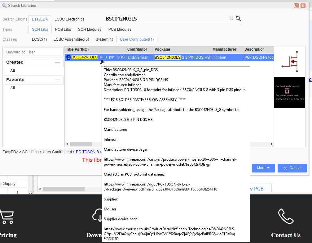
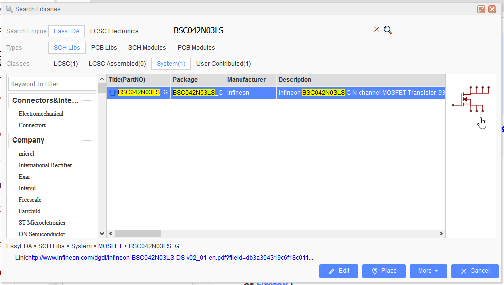
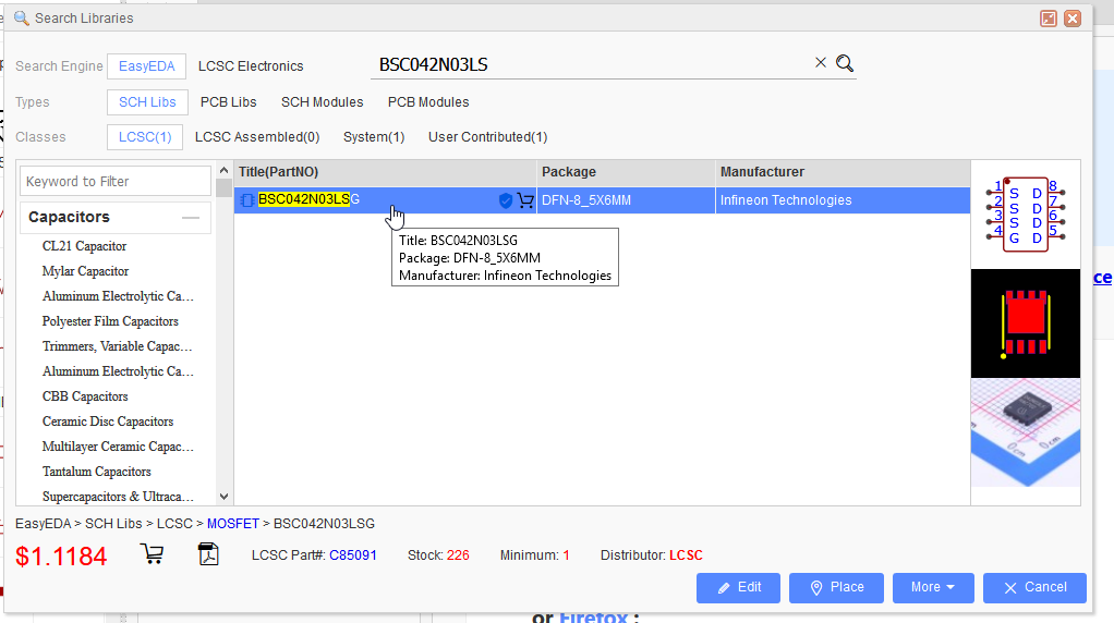
Also, search for
BSC042N03LS
and then analyse and compare the three symbols and footprints:
As a 3 pin symbol mapped onto an 8 pad footprint:
As an 8 pin symbol that has to be mapped onto an 8 pad footprint:
As an 8 pin symbol mapped onto an 8 pad footprint:


 Brand new interactions and interfaces.


 Easy to use and quick to get started.