You need to use EasyEDA editor to create some projects before publishing
How to combine same PCB footprints into one?
1668 9
Natanaelprado 3 years ago
Hi guys, it's me here again. So now I'm almost finishing my PCB layout, but I found that some components that were separated in my schematics got separated in the PCB layout too when I've converted. In fact, they are the same component but in my schematics, they were separated just to be more organized. But I don't know how I can combine these PCB footprints into one unique footprint. The image below shows the component 74AHC125, In my schematic it was divided into 4, but in reality, they are one, so I think that the program didn't understand it. ![Captura de tela de 2020-07-24 13-12-52.png](//image.easyeda.com/pullimage/VlmbFibKsHmj16vusxV4LG1C4W1q1zaxeoLUuoU0.png) 
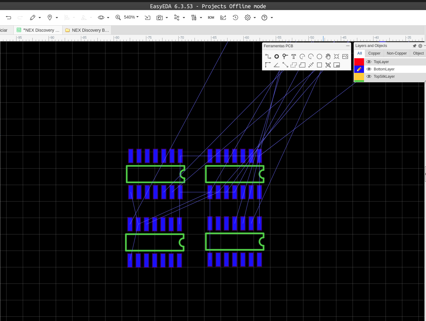
I tried to put one footprint on top of another, but this doesn't make the footprints turn into one and the yellow "X" appears because it's overlaid. So what I can do to solve it? ![Captura de tela de 2020-07-24 13-11-58.png](//image.easyeda.com/pullimage/iAFYe4C0Pwjaf6dCUCjnp4Dv2SxW9ReNvHK7gaF2.png) 
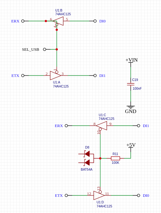
This is the schematic of this component. ![Captura de tela de 2020-07-24 13-57-42.png](//image.easyeda.com/pullimage/fXqEmCHvyX0ELRieGTo9fC0Kh8zg0JjZGjTUEhaA.png)
Comments
andyfierman 3 years ago
U1:B has a short between pins 4 & 6.
Reply
andyfierman 3 years ago
The reason you have 4 separate packages is because you have used an incorrect syntax for the prefixes. It is Um.n  where m = the package number              n = the number of the device in package m. So for example, the device you have prefixes as: U1:B should be written as: U1.2 Please take care to read the Tutorial and other documentation carefully to help yourself to avoid making mistakes. :)
Reply
Natanaelprado 3 years ago
@andyfierman OK. Thank you so much for spotting my mistake. So can I correct my schematics and update my PCB layout without losing my progress in the PCB Layout?
Reply
andyfierman 3 years ago
I have no idea what will happen to your PCB layout since you have not posted a link to a public copy to see it.
Reply
Natanaelprado 3 years ago
@andyfierman This is my PCB Layout... [https://easyeda.com/Natanaelprado/nex-discovery-board](https://easyeda.com/Natanaelprado/nex-discovery-board)  I've updated my schematics now with the correct syntax for the prefixes, the only thing I need is to update my PCB Layout footprints.
Reply
andyfierman 3 years ago
@Natanaelprado, Clone your project then try doing **Update PCB...**  on that and see what happens.
Reply
andyfierman 3 years ago
Yes, that will work OK and will not trash your PCB layout. BUT... If only people would read the documentation we provide before they launch into fantastically complex projects without having understood how to use the tool. Before you first converted your schematic to PCB you did not run, check, investigate and correct the many net errors and warning that exist. You did not terminate any unused pins with the green Unconnected Pin X symbol so they are all still confusing the Design Manager by loafing about as "net has less than two connections" warnings. Until you sort out the schematic and therefore the Design Manager warnings and get all the nets sorted (if there are 100 nets then it should show 100/100), you cannot rely on the PCB being correct to what you intend the schematic to represent. In other words you do not know if the connectivity of the schematic is complete. Then go through the checklist in (4) in (2) in: [https://easyeda.com/forum/topic/How-to-ask-for-help-and-get-an-answer-71b17a40d15442349eaecbfae083e46a](https://easyeda.com/forum/topic/How-to-ask-for-help-and-get-an-answer-71b17a40d15442349eaecbfae083e46a) Then you must do the same with the PCB Design Manager: * all the components present (the number shown in the PCB Design Manager = the number in the Schematic Design Manager)' * all the nets must show up as complete (no white cross on red background); * no DRC errors. Then go through the checklist in (6) in (2) in: [https://easyeda.com/forum/topic/How-to-ask-for-help-and-get-an-answer-71b17a40d15442349eaecbfae083e46a](https://easyeda.com/forum/topic/How-to-ask-for-help-and-get-an-answer-71b17a40d15442349eaecbfae083e46a) Then you can run the Gerbers, check them using gerbv and complete the checklist (6) above. Then check everything again. Then submit the board for manufacture after reading the instructions at the bottom left of the JLCPCB submission page.
Reply
Natanaelprado 3 years ago
Yes... It worked, Now the PCB Layout is updated with one unique footprint for each component. Thank you :) One more question. Do you think that my track width and clearance are ok to the manufacture? I mean JLCPCB machines can do it or it's too near to each one? including vias...
Reply
andyfierman 3 years ago
Check this page: [https://jlcpcb.com/pcbAssembly](https://jlcpcb.com/pcbAssembly)
Reply
Login or Register to add a comment
goToTop
你现在访问的是EasyEDA海外版,使用建立访问速度更快的国内版 https://lceda.cn(需要重新注册)
如果需要转移工程请在个人中心 - 工程 - 工程高级设置 - 下载工程,下载后在https://lceda.cn/editor 打开保存即可。
有问题联系QQ 3001956291 不再提醒
svg-battery svg-battery-wifi svg-books svg-more svg-paste svg-pencil svg-plant svg-ruler svg-share svg-user svg-logo-cn svg-double-arrow -mockplus- -mockplus- -mockplus- -mockplus- -mockplus- -mockplus- -mockplus- -mockplus-@1x -mockplus-

Cookie Notice

Our website uses essential cookies to help us ensure that it is working as expected, and uses optional analytics cookies to offer you a better browsing experience. To find out more, read our Cookie Notice