

Hi all,
I am designing a module that contains a li-ion charging module, battery protection, voltage booster, and latch switch. I have designed and fabricate the module but it seems not stable. Can anyone suggest what did I do wrong in my design? and how to improve it. I'm suspecting the latch parts has the issue as I ground it from Bat-. 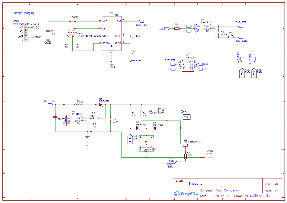


 Brand new interactions and interfaces.


 Easy to use and quick to get started.