I have terminals, which should be on PCB just a small copper areas, to solder external wires. But those are still shown in BOM, and that's confusing. Is it possible to hide those from BOM?
It is difficult to advise on all the possibilities without seeing your particular application.
Can you share the project, or an example that includes these pads, publicly?
Or if you have used pads such as 10MMPAD from - or have created your own and saved them to - the library: can you post their urls?
Are they pads like 10MMPAD that have been represented as Schematic Symbols in the Schematic and so will be pulled into the PCB when you did **Convert to PCB...**?
[https://easyeda.com/speed/AC-speed-control-for-grinder](https://easyeda.com/speed/AC-speed-control-for-grinder)
See P2, P3, P4, P5. Those exists on PCB as pads with holes, but should not exist in BOM.
@puzrin,
Except by manually deleting these lines from the exported BOM file, it is not possible to completely remove the entry for these parts from the BOM.
* It _is_ however, possible to remove all except their name, package and prefix number information and to show them as not being fitted to the PCB.
From the information in your schematic, it looks like you have created the Schematic Symbols for P2 - P5 yourself (Contributor: Speed Controls).
In the more recent versions of EasyEDA the developers have tried to make it easier for users to make their own Schematic Symbols by providing a template with fields for the part number, supplier and supplier part number. These fields are set with a default such that they will appear in the BOM even if left blank and it is not possible to simply delete them in the right hand panel in the Editor window.
* For Schematic Symbols that you have created however, it is possible to remove these fields so that they do not appear in the BOM.
Here's how:
Find the symbols in the Search Libraries tool (SHIFT+F search).
Select and Open them for editing in the Schematic Lib Editor.
Then for each one, do:
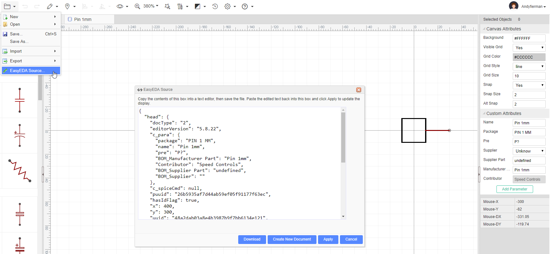
**Document > EasyEDA Source...**
Look closely at the first section of the file:

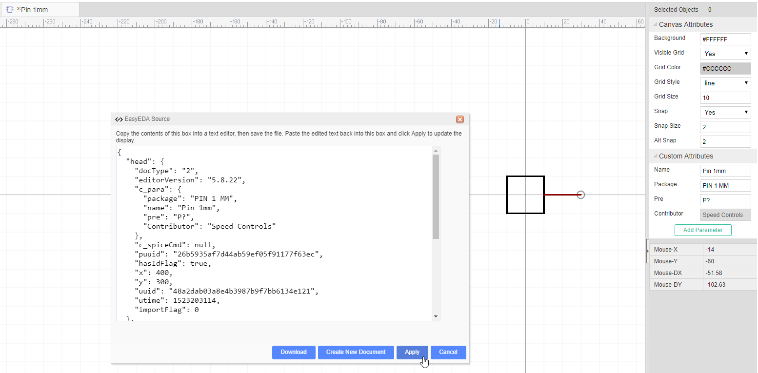
The lines starting "BOM_..." are the ones that make the information appear in the BOM so deleting them will remove that information from the BOM **BUT** for the syntax to remain correct, you must also keep the indentation and delete the "," at the end of the "Contributor" line.
Then click apply and save the edited symbol.
So, after editing the first section must look like:

Note that only "Name", "Package", "Pre" and "Contributor" now appear under "Custom Attributes".
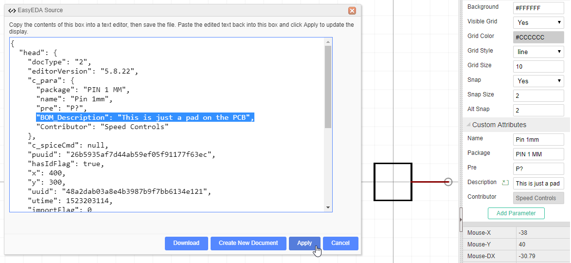
You could if you wish add an extra line, above the "Contributor" line to state in the BOM something like "This is just a pad on the PCB":

* Lastly, in the Schematic, for each P2, P3, P4 and P5 symbol set the **Mounted** attribute to **No**.
Thanks! That seems to work, but i got another issue instead. If i mark element as "not mounted" i see big red "(R)" marker below, in editor.
See P6 [https://easyeda.com/speed/AC-speed-control-for-grinder](https://easyeda.com/speed/AC-speed-control-for-grinder) (open in editor)
Is it possible to hide such marker or make is less annoying at least?
Our website uses essential cookies to help us ensure that it is working as expected, and uses optional analytics cookies to offer you a better browsing experience. To find out more, read our Cookie Notice