Hey all,
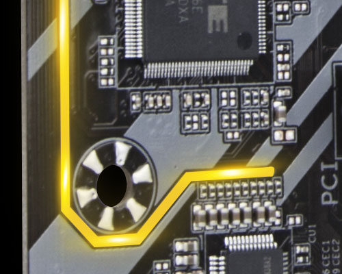
I'm trying to figure out if it's possible to design a PCB with exposed bare board material in the EasyEDA editor. My use case its that I would like to route simple 2mm or so trace width designs into the top and bottom of the board, with no solder mask or copper area in order to allow lighting to shine through the PCB from underneath. Strange use case, but I'm trying to mimic this feature as found on some Computer Motherboard PCBs, like shown here-


I know this is a gimmicky feature, but it's neat and could be fun for some projects.
<br>
Is there an easy way to make the trace into a bare board zone, like a "keep away" area to keep copper and soldermask out? If I could simply route a trace and then convert it into a keep-away zone it would be ideal.
Chrome
113.0.0.0
ChromeOS
14541.0.0
EasyEDA
6.5.23

