So, one more time about my task.
There is no schematics at all. I want to design just power distribution board.
The board has custom shape. It is double side. The most space of the PCB should be fill by copper. Some closed contours will be free from copper. There will be also some pads on both side.
That simple as idea, but have no idea how to do it.
I was trying to use Solid Region to fill all this shape. But gerber says ther are 1 000 000 errors ( DCR errors I guess).
..... So , please advise how to solve this simplest task in idea, which seems absolutely not simple using this soft.
Thank You in advance
So, the red is areas with copper, the black - without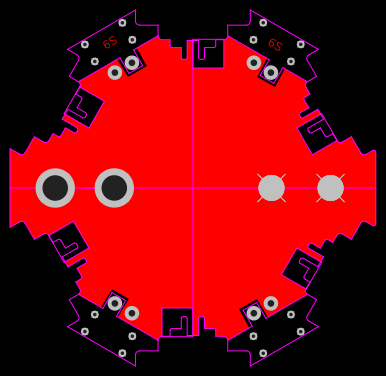
You seem to have got as far as creating the board outline (the purple line defining the outside edge).
You have also placed some pads and a couple of holes.
Questions:
Are top and bottom copper areas to be connected together?
do you care how many of these holes in the board are in electrical contact with the top and/or bottom copper area?
If yes must any of them be insulated from it?
If yes then from top or bottom or both?
How much clearance do you need around the ones that do have to be insulated from the copper area (to allow for screw heads, washers, nuts etc.)?
Simply draw a **Copper Area** around the whole board. It does not have to follow the board outline: can be a simple rectangle with all of it outside the board outline.
Set the Net attribute of the top and the bottom copper areas to some name: if they can be or you want them connected together then make the names the same (for example GND). If you want them unconnected to each other then give each area (top and bottom) different names (for example, A and B)
For simple non-plated-through holes use the **Hole** tool.
For plated through holes that can be used to join top and bottom copper together then use the Pad tool to create circular pads (set to **All Layers**) with specified outer copper and inner hole diameters. Set the **Net** attribute of each pad to the name of the copper area to which you want them connected (GND if it's OK for the two sides to be connected or if the two sides must be unconnected then A or B).
If you want the pads to create a clearance for things like washers but to not be connected to either copper area then leave the **Net** attribute of the pad blank and set the outer diameter to be greater than the washer diameter plus any tolerance on the washer positioning due to the bolt tolerances etc.
For a pad to be connected to a copper area, you can specify that the pad be connected to the copper area either **Directly** or by a **Spoke** using the **Pad Connection** property of the selected Copper Area.
Thank You a lot for Your detailed answer. I appreciate Your intention to help.
As for Your questions.(By the way, shown board is not finished)
1\. TOP and BOTTOM sides of the PCB should not be connected \! The TOP side is PLUS and the BOTTOM side is MINUS\.
2. As You can see there are 4 sections (2 upside of the PCB and 2 downside of PCB). Each section has 6 holes. Little D=1 mm holes (4 pieces) are isolated pads just for hold the part (XT 30 type connector). and other 2 pads are for actual soldering of the XT connector contacts. As You see, this pads are isolated from each other, because one will be soldered to the TOP side of the board , and the other will be soldered to the BOTTOM side of the board.
3\. 4 big Pads on the central part are 2 pairs 6\.5 mm bullet banana connectors\, and they will be also connected to the opposite sides of the board \( the design is not finished yet\, so You can't see it\)
I already find out how to fill the board with the copper and how make islands :). Anyways thanks for explanation.
Although , it is very pity, that program has no options for different shapes for the solid areas. There is no possibility to cut off the round (circle) shape and it is shame. So I have to draw just rectangular areas and it is not always convenient.
Otherwise nice program.
It is fiddly but you can draw any shape with the Solid Region.
1. Click, drag and click to define the initial shape.
2. Then click and drag on the blue circles in the region outline to add new vertices,
3. Double click on the green circles to delete vertices.
@andyfierman, Yes, you are right. You can draw any shape (any triangular, square.....), any shape which has a corners, but you really can not draw fine circle.
But I am still interested in 2 points:
1\. Possibilities to draw circles\, as copper cut off areas\. May it is possible to make everything in this soft\, and when transfer the gerber file to another soft \, make circle cut offs there\, save as gerber file and transfer it back to the easyeda?
2\. As I realize\, You use some kind of CNC machines to cut the edges of the PCB and make holes\. But there is no possibility to make a square hole\, or any shape hole\. Why? Is it so difficult to have this option? For example to have a possibility to cut the hole by the shape\, imported from DFX file?
I think that this 2 options will make Easyeda the best !!!
As I said, it is fiddly but you can make a pretty good approximation to a circle by adding and adjusting the vertices of a Solid Region outline.
About your points:
1\. You can edit your Gerbers using external software \(although I am not aware of any free software that will allow you to do that\) and then upload them into the JLCPCB PCB submission page\.
2\. You can make a hole of any shape in the PCB using the **Solid Region** tool set to "NPTH". You can also import a DXF file into EasyEDA.
For more please see the Tutorial.
Our website uses essential cookies to help us ensure that it is working as expected, and uses optional analytics cookies to offer you a better browsing experience. To find out more, read our Cookie Notice


 Brand new interactions and interfaces.


 Easy to use and quick to get started.