
In general each CMOS part (microprocessors, logic gates, optocoupler) needs a small capacity (mostly 100nF) between their +5V/+3.3V input (voltage supply) and ground.
The pads of this decoupling capacity have specially designed from the outer four corners to fence the disturbances (produced by the working CMOS circuit) in the inner loop
(see the following pic - you can skip the German explanations :-)
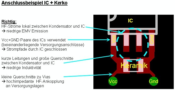
(source [http://www.lothar-miller.de/s9y/categories/14-Entkopplung](http://www.lothar-miller.de/s9y/categories/14-Entkopplung))
But how to implement this design in EasyEDA?
(1) simply connect the pad of the decoupling capacity to GND gives you more than the one in the cormer in present of a surrounding GND copper area!
(2) give the pad a new name (aka build a new net) - for example GND-CMOS - and then, connect GND-CMOS to GND does even not work since EasyEDA unifies both nets and you have the problem as given in (1)!
(3) simply give the pad a new name and skip the connection to the general net GND in the schematics and instead simply draw this connection in the PCB works but raises of course a "Track to PAD" DRC Error!
Is there a solution in EasyEDA to exactly model the drawn decoupling capacity without any DRC error?


 Brand new interactions and interfaces.


 Easy to use and quick to get started.