You need to use EasyEDA editor to create some projects before publishing
Incomplete PCB Connections Errors
3522 28
JulesP 4 years ago
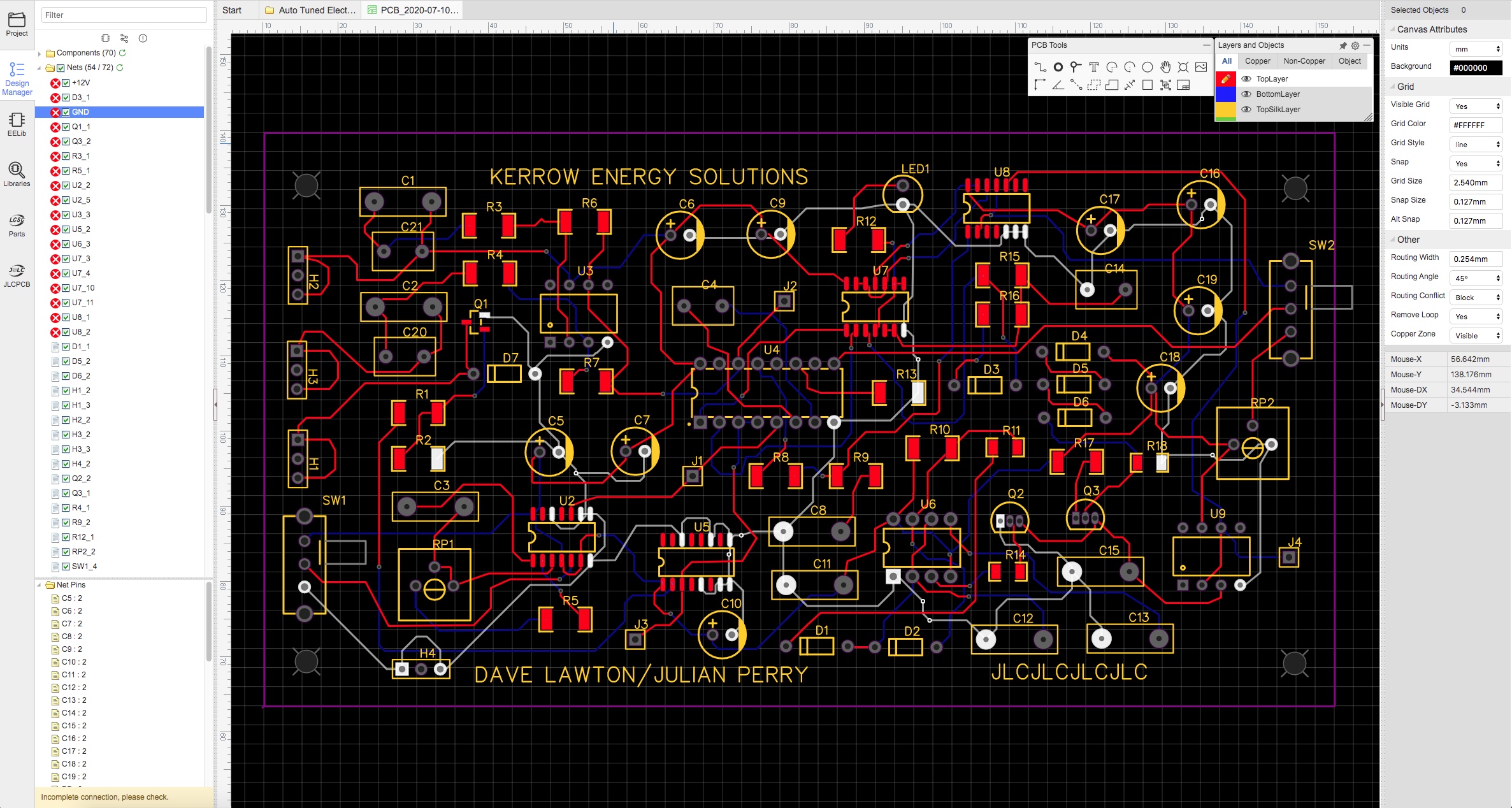
I have just completed a PCB design and did the circuit check before producing the Gerber files. It came up with a whole load of 'errors' based on 'incomplete connections'. I don't understand this as all the connections are as the schematic says and, in the case of the highlighted GND one, they all connect to each other and to the GND terminal at H4 in the lower left corner. What am I missing here or is this as assumed error based on a set of circuit assumptions? Thanks Jules ![PCB QUERY.jpeg](//image.easyeda.com/pullimage/eNgab3a0pAiTi2dNtEmBAXImAxTYE8CKwaYr3GTs.jpeg)
Comments
andyfierman 4 years ago
Without access to your whole project it is difficult to diagnose exactly what has gone wrong but the underlying problem is the same as in your earlier post about incomplete or broken PCB connections. You are not paying enough attention to the connectivity in your schematic and the subsequent creation and updating of your PCB. If you get the connectivity correct in the schematic - and to help this we recommend naming your nets -
Reply
andyfierman 4 years ago
 then the connectivity of the PCB will be correct to the schematic. Proper use of the Design Manager - and going through the Checklists - throughout the schematic and the PCB design process rather than just at the end will help you find and correct errors before you get to the overwhelming stage you're at right now at what you thought was the end of the PCB design.
Reply
JLCPCBsupport 4 years ago
Hello ; As @[andyfierman](https://easyeda.com/andyfierman) says already without having access to the project helping you will be a kind of "guessing game" so please to share the "public" link to your project to check the schematic. meanwhile let's guess, I think that you are using ICs and components and missing the connection of "un-used pins" like for example when someone use a MCU and don't connect all its pin just the necessary ones so the rest of pins will appear as missed connection errors once you leave them with no connection so I advise you to put a "no connect flag" from the wiring tool palette right on the not used pins. ![no connect flag.JPG](//image.easyeda.com/pullimage/lS9isyZZ9J5Ne3nscu1jjTBPPbad77wutCKnUuFT.jpeg) Please share the link to your project in order to help you better.
Reply
andyfierman 4 years ago
Looking at the PCB design it looks like you are designing a commercial product. As such there are a number of aspects that appear less than ideal even without sight of your original Design Requirements Spec or the schematic. 1) There are several groups of capacitors that would appear to be supply decouplig but which are lumped together in no obvious relationship (i.e. proximity) to the devices which they are supposed to be decoupling. They appear to be grouped according to convenience of placement rather than efficacy of function: ![image.png](//image.easyeda.com/pullimage/fzler3z3n9JHbMZtcTL9Wpn8s37UChz7nrV3uTpB.png) The correct placement of components, particularly decoupling capacitors, in a PCB is discussed in (2.2) in (2) in: [https://easyeda.com/forum/topic/How-to-ask-for-help-and-get-an-answer-71b17a40d15442349eaecbfae083e46a](https://easyeda.com/forum/topic/How-to-ask-for-help-and-get-an-answer-71b17a40d15442349eaecbfae083e46a) 2) The layout is very open with long meandering traces between devices. 3) There is no clear up/down, left/right routing regime beween the top and bottom layers to minimise coupling between crossing traces. 4) Ground and supply tracks are unnecessarily narrow, being the same width as what are assumed to be low current signal traces. 5) There appears to be no use of a ground or any power planes. The combination of a large open layout and a total abscence of at least a Copper Area to create a ground plane ideally on the top layer, and preferrably the use of Copper Areas to provide a low ground and supply impedances and to help with shielding the traces from radiated interference (EMI), is an EMC disaster waiting to happen. A more compact layout with more thought to the component placement and routing will improve the effectiveness of the supply decoupling, possibly requiring less and so reducing component and assembly costs, will reduce the loop areas represented by the various track runs, assisting in reducing the susceptibility to EMI and will also reduce the board cost. Adding at least a ground plane with better routing can significantly reduce susceptibility to EMI. Adding power planes can also contribute to improved susceptibility. Both can help ease routing contraints because the ground and supply nets no longer need to be explicitly routed. An additional effect of adding both ground and power planes is that it can improve the copper balance between top and bottom layers and so reduce the tendency of boards with imbalanced copper to warp. The use of mixed SMD and through hole parts increases assembly costs. It might be worth considering an all SMD design that you can get assembled at lower cost.
Reply
JulesP 4 years ago
@andyfierman Hi there, This is a personal project not a commercial production. I’m not sure yet how to share but will have a look soon to do so. Is that a share with you specifically or to anyone? I do use the checklists and the earlier ‘errors’ didn’t make sense either and it advises one to ignore them if one has designed it that way. I thought a large copper area would take up lots of space and while I recognise the need to increase the track width for the ground and power tracks there should be no more than 2A flowing in them so I assumed it was not urgent. Where do you think EMI would come from in this case? I have mixed SMD and THT because if a chip fails then it’s easier to swap out from a chip holder than desolate all the pads of an SMD. Julian
Reply
JulesP 4 years ago
@JLCPCBsupport Yes that would be useful to do.
Reply
JulesP 4 years ago
@andyfierman I’ve checked connectivity extensively but possible am confused by the need or not to see a red dot when a component is joined either side by a connection. In those situations a red dot does not appear but only at junctions and apparently end points on terminals for example. Anyway as the thin blue lines In the PCB layout were all in place at the start and the tracks and pads became highlighted when part of the track was touched then that indicated that there were sound connections - doesn’t it?
Reply
JulesP 4 years ago
@andyfierman I'm using the client on a Mac. Is there a share option from that? I haven't found it yet. If not can I export it to you? J
Reply
JulesP 4 years ago
@andyfierman I can't see anything about cap placement in the link you gave. It's all about using the forum.
Reply
JulesP 4 years ago
@andyfierman OK I have exported the relevant files to the Online version and set it up on there but it won't let me share a link saying'My time on EasyEDA edit is too short to allow this'!!
Reply
JulesP 4 years ago
@andyfierman Andy, I have managed to get a link to include you as a member. [https://easyeda.com/join?type=project&key=0ccc0ba6d6297f4460b04865733671e2](https://easyeda.com/join?type=project&key=0ccc0ba6d6297f4460b04865733671e2) Seems to be the only way at the moment, possibly because I have only just transferred this project from the client to the online version.
Reply
andyfierman 4 years ago
How to share? You know what I'm going to say don't you? Please read the Tutorial (1) in (2) in: [https://easyeda.com/forum/topic/How-to-ask-for-help-and-get-an-answer-71b17a40d15442349eaecbfae083e46a](https://easyeda.com/forum/topic/How-to-ask-for-help-and-get-an-answer-71b17a40d15442349eaecbfae083e46a) :) "Where do you think EMI would come from in this case?" Where do you think? I have no idea what you circuit is used for or in what environment it is intended to operate. Mains hum; AM radio; Taxi and public service radio; Wifi from your hub; Your mobile phone; Switch mode supplies in lousy cheap laptop supplies and wall warts. The amateur radio station next door but one; Those Ethernet over The Mains adaptors; The kid on the moped with the unsuppressed spark plug cap; Shifting about on the office chair; Shuffling a pocket full of loose change. The list is endless. (See this for the last two in that list: [http://emcesd.com/pdf/uesd99-w.pdf](http://emcesd.com/pdf/uesd99-w.pdf)) EMI happens. It's a fact of life. You don't get any say in which particular form of it is going to arrive and mess with you circuit and therefore whatever is connected to it (Think about the consequences of that very carefully). You only get a red do at the junction of 2 or more wires. Wires to symbol pins should never show a red dot. If it does it means you have overshot the end or are passing across it at an angle (usually 90deg which can be dangerous as you may short to other pins in the same row or column). As advised in (2.2) in the Welcome to EasyEDA link, do not join 3 wires at a cross: stagger then so it is clear that they are joined deliberately and it's not an accident whilst crossing 2 wires. When you draw a schematic what you are doing is creating a netlist of the connectivity using a graphical tool. When you convert to PCB all that happens is that the schematic netlist is passed - and all the PCB Footprints assigned in it are pulled - into the PCB Editor and connected up according to the connectivity defined in the schematic. You have to get the connectivity right in the schematic for it to be right in the PCB. If there's a mistake or change, you cannot fix it in the PCB because then the netlists of the schematic and the PCB are different. It must be changed in the schematic and then passed into the PCB by Update PCB or Import Changes. Attempting to make changes to the connectivity in the PCB will result in net naming errors because there will then be nets in the PCB that do not exist in the schematic. You can still get incomplete net errors in the PCB if you have nodes (pads and end points of tracks) that are unconnected simply because there are some as yet unrouted parts of the net on the PCB. I suspect this is a bug but you do need to be aware that if for whatever reason you change the net names in the schematic, when you next do an Update PCB or Import Changes, there may be some orphaned segments of ratline or track that can end up with the wrong net name on them. I have encountered this a few times recently but they are easy enough to find using the Design Manager and then to fix in the PCB editor by renamining the affected pads and track segments to the correct netname.
Reply
JulesP 4 years ago
@andyfierman I tried to share ( I do know how) but it would not let me as I had only just loaded my project onto the online system. I was prevented but I posted a link as an alternative for member inclusion. Details of what my project is for is in the online version (electrolyser pulsing system) I have sorted all the errors which were due to my using Netlabels instead of the Text labels and so were not due to connectivity issues (as I thought). I've taken great care over that but my use of Netlabels confused the system. My only outstanding issue is the inclusion of a copper ground pad I think its called. Also perhaps the new component placement feature you reviewed may produce a better more track efficient placement?
Reply
andyfierman 4 years ago
" I can't see anything about cap placement in the link you gave. It's all about using the forum." No it isn't. "...(2.2) in (2) in: [https://easyeda.com/forum/topic/How-to-ask-for-help-and-get-an-answer-71b17a40d15442349eaecbfae083e46a](https://easyeda.com/forum/topic/How-to-ask-for-help-and-get-an-answer-71b17a40d15442349eaecbfae083e46a)" means reading this: ![image.png](//image.easyeda.com/pullimage/FQZI3KIm4HZvds3oaIlFaJE2gEpE2oFOBMKbxsi9.png) which links to this: ![image.png](//image.easyeda.com/pullimage/0lpnNtPERLHgS8t5hQ0QNIQWXzK06mvbZJPsygM4.png) 2.2) [How to design PCBs](https://docs.google.com/document/d/1CU7RuPyFlSZPzWBN-YZ0x87xeAB4xpLdLaIsUwhLj_M/edit?usp=sharing) where you'll find: "## What is PCB Design? One of the mistakes made by people new to PCB Design is to simply group things like all the decoupling capacitors together into one area, all the resistors in another and all the ICs in yet another area and then connect them up with copper tracks. This might make the component layout look tidy but that is not what PCB Design is about. ****PCB Design is about placing components as close to where they need to be to do the job that they have been included in the schematic for as the physical constraints of whatever enclosure it is to be housed in will allow, taking into account factors such as PCB dimensions, component height clearances and enclosure materials**.**" Decoupling capacitance is descussed in several subsequent sections. If you don't understand what it is referring to in there then please see this: [https://easyeda\.com/andyfierman/Power\_supply\_decoupling\_and\_why\_it\_matters\_\-451e18a0d36b4f208394b2a2ff7642c9](https://easyeda.com/andyfierman/Power_supply_decoupling_and_why_it_matters_-451e18a0d36b4f208394b2a2ff7642c9) I just don't have time to teach this stuff so if you need more information about the correct application of power supply decoupling then read the device datasheets for guidance. There's a lot of good info about this in the device manufacturers' sites. Places like Analog Devices, TI and OnSemi have reams of the stuff. Ditto on PCB layout, EMC, SI and PI.
Reply
JulesP 4 years ago
Opps they have come back again, the connection errors but not the other labelling ones. I can't honestly see any distinction between the good ones and the bad ones. I've used the same process to make them. Check the schematic again I guess. J
Reply
JulesP 4 years ago
I have just checked the connections re one of the errors which is just a short link between a diode and a resistor (D3) and there's nothing wrong with it and I've updated the PCB which says no changes. So why is there a connection error? What rationale is it using for saying there is? Thanks for all your efforts by the way. J
Reply
andyfierman 4 years ago
OK, I know what's wrong. I think you really, really, really need to do as we advise and create yourself a simple project to play with and get used to using the tool before launching into a more complex project like this one. Here's a screenshot of part of your board. There are 5 incomplete connection in it plus the marked DRC error of two tracks too close together. ![image.png](//image.easyeda.com/pullimage/qd7apPw0eYOJb2GEegz1eVU3Ef2anBj23FBtLMXG.png) The incomplete nets are all due to the same mistake. Here's a close up of one of them: ![image.png](//image.easyeda.com/pullimage/3dmbcevcSwa6fny8IPmphnZbWXvl2WSiKtUd5Kt2.png) Can you see it yet? You're going to hate me when I point it out. :) : : : : : You cannot connect to a pad on the top layer by routing a trace to it on the bottom layer. Now, go grab a tea and a bun, watch some rubbish telly and sort it out in the morning. :)
Reply
GerritMax 4 years ago
I've experianced the same errors, really zoom in to the connections that give an error and you'll see a tiny bit of ratline.
Reply
andyfierman 4 years ago
@GerritMax, Well spotted: ![image.png](//image.easyeda.com/pullimage/frkQgKU6BGP6sIYIorJumhef7JMf6ntU9gbZOLVl.png) although only if the pad and track snap vertices are offset from each other. However, with this particular type of incomplete connection the error, once realised, each instance hardly needs to be zoomed in on in to be seen and checked.
Reply
JulesP 4 years ago
I see what you are saying. Telly was indeed rubbish. I did do a timer circuit for my first PCB and went through the whole process to production and learnt a lot. Without zooming big time my connections looked like they were complete. Isn't there a snap to feature for this as when you start a track it snaps to the start point no problem? In this grab you can see a small bit of ratline left but no amount of moving the track endpoint will get rid of it since if I move the green dot to the right it jumps over to what's shown in the second grab\. In other words no amount of moving the track end will make all the ratline disappear\. I'm sure there's a simple answer :\| ![PCB Query 1.jpeg](//image.easyeda.com/pullimage/31YhiqRfYt2MKRuT5jQfEy5olaUn1AXBdsaiITLF.jpeg) ![PCB Query 2.jpeg](//image.easyeda.com/pullimage/BecyKIlv6IZ2GZsMbzf4kIlDcA9UfvKPXbhcFVEB.jpeg)
Reply
JulesP 4 years ago
I guess this is one of those top vs bottom layer issues.
Reply
JulesP 4 years ago
Ok I can see how to resolve all these. Thanks again.
Reply
andyfierman 4 years ago
@JulesP, From your comments this morning I just want to be sure you understand the problem you had. If you have a pad on one layer, you can **only** connect to it by routing a track to (or from) it **on the same layer**. So if you have a pad on the one layer, and a track on a different layer **you** **have** **to** **transfer** **the** **track** **to** **the** **same** **layer** **as** **the** **pad** **using** **a** **via** (using the really neat process as explained in the Tutorial). Obviously this does not apply to multi-layer (through-hole) pads because they have pads on all layers and through-hole plating that connects them all together.
Reply
JulesP 4 years ago
Yes, I finally got there. In the interests of efficiency, I had it in my head that I should keep vias to a minimum so avoided using another to bring the track back up to the top layer and so the track would not connect to the pad. I have now been through all the error connections and they are all gone now. I have also done the Copper Pour for GND and to reduce EMI and had a think about decoupling cap placement. In fact when I used the Cross Probe and Place option it opted to put them in roughly the same general areas I had done so I returned to my earlier version and refined that. I'm sure the more expert PCB designers would have things to say about extended tracks, the space I have used and mixing SMD/THT but my PCBs will be infrequent and my frequency in operation will be
Reply
JulesP 4 years ago
. . . < 10kHz. Thanks for the nudging :) ![PCB Layout 2A.jpeg](//image.easyeda.com/pullimage/s9zpdSLZjoJMSivDdJTlDrZ5YpkxjVuekdp2HbTC.jpeg)
Reply
andyfierman 4 years ago
@JulesP, As you mentioned it: "...frequency in operation will be < 10kHz" A common misconception about Signal Integrity and to a slightly lesser extent, EMC is that it's the frequency of the oscillators, clocks and pulse generators that matters: if they are low enough there won't be any SI or EMC issues. It's not the frequency. It's how fast the edge transitions are. You can have a clock period of once a fortnight but of the edges are 1ns ride anfall times and the layout causes enough crosstalk that of a rising or a falling edge kicks a reset line then once a fortnight, every fortnight: that circuit will reset. To a large extent your circuit uses devices that have slow enough edge transitions that you may not have any problems but if you are dealing with low level signals then you may need to consider possible sources and effects of crosstalk in the layout One last comment about decoupling caps. U5 is a bipolar technology 555 timer. You **must** decouple it at the device supply pins. So put C18 close to U5. The project: [https://easyeda\.com/andyfierman/Power\_supply\_decoupling\_and\_why\_it\_matters\_\-451e18a0d36b4f208394b2a2ff7642c9](https://easyeda.com/andyfierman/Power_supply_decoupling_and_why_it_matters_-451e18a0d36b4f208394b2a2ff7642c9) explains and demonstrates why and the LM555 datasheet: [https://www.ti.com/lit/ds/symlink/lm555.pdf?ts=1594591206045&ref_url=https%3A%2F%2Fwww.google.com%2F](https://www.ti.com/lit/ds/symlink/lm555.pdf?ts=1594591206045&ref_url=https%253A%252F%252Fwww.google.com%252F) is quite explicit in the section 10 Layout and in Fig 20.
Reply
JulesP 4 years ago
Ok, done re C18. I noted when I built my fully adjustable timer using two 555 that it is not easy to get its output stable but I think this is just as much a matter of the stability of the timing capacitor as of the supply stability. ![U5 Decoupling.jpeg](//image.easyeda.com/pullimage/QVa4duEsoTNLXxMnTrNFnIff67Yjq3fwJf0lGVLn.jpeg)
Reply
andyfierman 4 years ago
@JulesP, Assuming that you're talking about the circuit in this: [https://easyeda.com/forum/topic/Broken-PCB-Connections-176f0fd913c84bda884b80b7634e032a](https://easyeda.com/forum/topic/Broken-PCB-Connections-176f0fd913c84bda884b80b7634e032a) it could be you have a noisy pot (or, less likely, unknowingly used a Y5V dielectric ceramic 10nF timing cap) but my money is on the lack of local decoupling on either of your 555 timer chips. You can prove it easily enough by soldering a 100nF cap directly across pins 1 and 8 of both 555 timers. The guy who designed the 555 timer knew it had a problem with shoot-through current and that is almost certainly why he put the GND and VCC pins at the same end. On that subject your C18 position is better but spinning it 180 deg would put the VCC end of the cap directly at pin 8 with the GND end at a low impedance route (via the copper plane) to ground. Spinning it 90 deg with the VCC end at pin 8 and the GND end at pin 1 would be perfect. Doing the same with the other chips would be even better and in particular placing C14 as close as possible to U3 will give the 4046 PLL a much easier life trying to stay in a stable lock. About ceramic cap dielectric materials: [https://www.edn.com/temp-and-voltage-variation-of-ceramic-caps-or-why-your-4-7-uf-part-becomes-0-33-uf/](https://www.edn.com/temp-and-voltage-variation-of-ceramic-caps-or-why-your-4-7-uf-part-becomes-0-33-uf/) Y5V dielectric nowadays is so bad it's just useless. About the man who designed the 555 timer: [https://www.electronicdesign.com/news/trends-analysis/article/21795268/the-555-timer-was-just-the-beginning-for-hans-camenzind](https://www.electronicdesign.com/news/trends-analysis/article/21795268/the-555-timer-was-just-the-beginning-for-hans-camenzind) I can recommend the download of the free pdf of his book from: [http://www.designinganalogchips.com/](http://www.designinganalogchips.com/)
Reply
Login or Register to add a comment
goToTop
你现在访问的是EasyEDA海外版,建议访问速度更快的国内版 https://lceda.cn(需要重新注册)
如果需要转移工程请在个人中心 - 工程 - 工程高级设置 - 下载工程,下载后在https://lceda.cn/editor 打开保存即可。
有问题联系QQ 3001956291 不再提醒
svg-battery svg-battery-wifi svg-books svg-more svg-paste svg-pencil svg-plant svg-ruler svg-share svg-user svg-logo-cn svg-double-arrow -mockplus- -mockplus- -mockplus- -mockplus- -mockplus- -mockplus- -mockplus- -mockplus-@1x -mockplus-

Cookie Notice

Our website uses essential cookies to help us ensure that it is working as expected, and uses optional analytics cookies to offer you a better browsing experience. To find out more, read our Cookie Notice